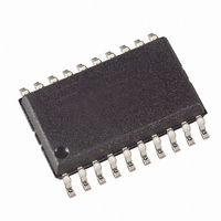
T5760-TGQ Atmel, T5760-TGQ Datasheet - Page 18

T5760-TGQ
Manufacturer Part Number
T5760-TGQ
Description
IC RX 868MHZ ISM ASK/FSK 20-SOIC
Manufacturer
Atmel
Specifications of T5760-TGQ
Frequency
868MHz
Sensitivity
-110dBm
Data Rate - Maximum
10 kBaud
Modulation Or Protocol
ASK, FSK
Applications
General Purpose Data Transmission Systems
Current - Receiving
7.8mA
Data Interface
PCB, Surface Mount
Antenna Connector
PCB, Surface Mount
Voltage - Supply
4.5 V ~ 5.5 V
Operating Temperature
-40°C ~ 105°C
Package / Case
20-SOIC (0.300", 7.50mm Width)
Operating Temperature (min)
-40C
Operating Temperature (max)
105C
Operating Temperature Classification
Industrial
Lead Free Status / RoHS Status
Contains lead / RoHS non-compliant
Features
-
Memory Size
-
Lead Free Status / Rohs Status
Not Compliant
Other names
T5760-TGQTR
Figure 23. Output of the Data Clock After a Successful Bit Check
Figure 24. Timing Characteristic of the Data Clock (Rising Edge on Pin DATA)
Figure 25. Timing Characteristic of the Data Clock (Falling Edge of the Pin DATA)
18
T5760/T5761
Dem_out
Data_out (DATA)
DATA_CLK
Serial bi-directional
data line
Data_In
DATA_CLK
Data_Out
Data_Out
Serial bi-directional
data line
Data_In
DATA_CLK
The delay of the data clock is calculated as follows: t
t
edge, t
resistor R
(see Figure 24, Figure 25 and Figure 32). When the level of Data_In is equal to the level
of Data_Out, the data clock is issued after an additional delay t
Note that the capacitive load at Pin DATA is limited. If the maximum tolerated capacitive
load at Pin DATA is exceeded, the data clock disappears (see chapter ’Data Interface’).
Delay1
'1'
Receiving mode,
bit check active
Bit check ok
is the delay between the internal signals Data_Out and Data_In. For the rising
Delay1
'1'
V
V
Il
Ih
pup
= 0,65 * V S
= 0,35 * V S
. For the falling edge, t
depends on the capacitive load C
'1'
V
X
'1'
t
Delay1
t
t
Delay
Delay1
t
Delay
'1'
t
Delay2
t
P_Data_Clk
t
Delay2
t
Data
P_Data_Clk
Start bit
'0'
Delay1
V
V
V
X
Ih
Il
= 0,35 * V S
= 0,65 * V S
Receiving mode,
data clock control
logic active
'1'
depends additionally on the external voltage V
'1'
L
at Pin DATA and the external pull-up
'0'
Delay
= t
'1'
Delay1
Delay2
'0'
+ t
.
Delay2
4561B–RKE–10/02
X


