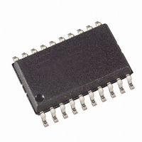
T5760-TGQ Atmel, T5760-TGQ Datasheet - Page 26

T5760-TGQ
Manufacturer Part Number
T5760-TGQ
Description
IC RX 868MHZ ISM ASK/FSK 20-SOIC
Manufacturer
Atmel
Specifications of T5760-TGQ
Frequency
868MHz
Sensitivity
-110dBm
Data Rate - Maximum
10 kBaud
Modulation Or Protocol
ASK, FSK
Applications
General Purpose Data Transmission Systems
Current - Receiving
7.8mA
Data Interface
PCB, Surface Mount
Antenna Connector
PCB, Surface Mount
Voltage - Supply
4.5 V ~ 5.5 V
Operating Temperature
-40°C ~ 105°C
Package / Case
20-SOIC (0.300", 7.50mm Width)
Operating Temperature (min)
-40C
Operating Temperature (max)
105C
Operating Temperature Classification
Industrial
Lead Free Status / RoHS Status
Contains lead / RoHS non-compliant
Features
-
Memory Size
-
Lead Free Status / Rohs Status
Not Compliant
Other names
T5760-TGQTR
Data Interface
26
T5760/T5761
Bit 15 is followed by the equivalent time window t9. During this window, the equivalence
acknowledge pulse t8 (E_Ack) occurs if the just programmed mode word is equivalent to
the mode word that was already stored in that register. E_Ack should be used to verify
that the mode word was correctly transferred to the register. The register must be pro-
grammed twice in that case.
Programming of a register is possible both in sleep-mode and in active-mode of the
receiver.
During programming, the LNA, LO, lowpass filter IF-amplifier and the FSK/ASK
Manchester demodulator are disabled.
The programming start pulse t1 initiates the programming of the configuration registers.
If bit 1 is set to ’1’, it represents the OFF command to set the receiver back to polling
mode at the same time. For the length of the programming start pulse t1, the following
convention should be considered:
•
Programming respectively OFF command is initiated if the receiver is not in reset mode.
If the receiver is in reset mode, programming respectively Off command is not initiated
and the reset marker RM is still present at Pin DATA.
This period is generally used to switch the receiver to polling mode or to start the
programming of a register. In reset condition, RM is not cancelled by accident.
•
Programming respectively OFF command is initiated in any case. The registers
OPMODE and LIMIT are set to the default values. RM is cancelled if present.
This period is used if the connected microcontroller detected RM. If the receiver oper-
ates in default mode, this time period for t1 can generally be used.
Note that the capacitive load at Pin DATA is limited.
The data interface (see Figure 32) is designed for automotive requirements. It can be
connected via the pull-up resistor R
The applicable pull-up resistor R
the selected BR_range (see Table 12).
Table 12. Applicable R
C
t1(min) < t1 < 5632 T
t1(min) is the minimum specified value for the relevant BR_Range
t1 > 7936 x T
C
L
L
£ 100pF
£ 1nF
-
Clk
pup
Clk
:
BR_range
B0
B1
B2
B3
B0
B1
B2
B3
pup
pup
depends on the load capacity C
up to 20 V and is short-circuit-protected.
1.6 k W to 470 k W
1.6 k W to 220 k W
1.6 k W to 120 k W
Applicable R
1.6 k W to 5.6 k W
1.6 k W to 47 k W
1.6 k W to 22 k W
1.6 k W to 12 k W
1.6 k W to 56 k W
L
at Pin DATA and
pup
4561B–RKE–10/02


