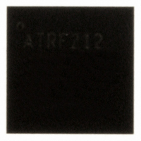
AT86RF212-ZU Atmel, AT86RF212-ZU Datasheet - Page 16

AT86RF212-ZU
Manufacturer Part Number
AT86RF212-ZU
Description
IC TXRX ZIGBE/802.15.4/ISM 32QFN
Manufacturer
Atmel
Datasheet
1.AT86RF212-ZU.pdf
(172 pages)
Specifications of AT86RF212-ZU
Frequency
700MHz, 800MHz, 900MHz
Data Rate - Maximum
250kbps
Modulation Or Protocol
802.15.4 Zigbee, 6LoWPAN, ISM
Applications
ISM, ZigBee™
Power - Output
10dBm
Sensitivity
-110dBm
Voltage - Supply
1.8 V ~ 3.6 V
Current - Receiving
9.2mA
Current - Transmitting
25mA
Data Interface
PCB, Surface Mount
Antenna Connector
PCB, Surface Mount
Operating Temperature
-40°C ~ 85°C
Package / Case
32-VQFN Exposed Pad, 32-HVQFN, 32-SQFN, 32-DHVQFN
Number Of Receivers
1
Number Of Transmitters
1
Wireless Frequency
769 MHz to 935 MHz
Interface Type
SPI
Noise Figure
7 dB
Output Power
21 dB
Operating Supply Voltage
1.8 V, 3 V
Maximum Operating Temperature
+ 85 C
Mounting Style
SMD/SMT
Maximum Supply Current
25 mA
Minimum Operating Temperature
- 40 C
Modulation
OQPSK
Protocol Supported
802.15.4
Operating Temperature (min)
-40C
Operating Temperature (max)
85C
Operating Temperature Classification
Industrial
Lead Free Status / RoHS Status
Lead free / RoHS Compliant
Memory Size
-
Lead Free Status / Rohs Status
Lead free / RoHS Compliant
Available stocks
Company
Part Number
Manufacturer
Quantity
Price
Company:
Part Number:
AT86RF212-ZU
Manufacturer:
HITTITE
Quantity:
5 000
Part Number:
AT86RF212-ZU
Manufacturer:
ATMEL/爱特梅尔
Quantity:
20 000
Part Number:
AT86RF212-ZUR
Manufacturer:
MICROCHIP/微芯
Quantity:
20 000
4.3 SPI Protocol
Table 4-2. SPI Command Byte Definition
4.3.1 Register Access Mode
16
Bit 7
1
1
0
0
0
0
AT86RF212
Bit 6
0
1
0
1
0
1
Bit 5
1
1
0
0
Bit 4
Referring to Figure 4-2 and Figure 4-3, MOSI is sampled at the rising edge of the SCLK
signal and the output is set at the falling edge of SCLK. The signal must be stable
before and after the rising edge of SCLK as specified by t
parameters 10.4.5 and 10.4.6.
This SPI operational mode is commonly known as “SPI mode 0”.
Each SPI sequence starts with transferring a command byte from the SPI master via
MOSI (see Table 4-2) with MSB first. This command byte defines the SPI access mode
and additional mode-dependent information.
Each SPI transfer returns bytes back to the SPI master on MISO. The content of the
first byte is the PHY_STATUS field, see section 4.4.
In Figure 4-4 to Figure 4-14 and the following sections, logic values stated with XX on
MOSI are ignored by the radio transceiver but need to have a valid logic level. Return
values on MISO stated as XX shall be ignored by the microcontroller.
The different access modes are described within the following sections.
A register access mode is a two-byte read/write operation initiated by /SEL = L. The first
transferred byte on MOSI is the command byte, including an identifier bit (bit7 = 1), a
read/write select bit (bit 6), and a 6-bit register address.
On read access, the content of the selected register address is returned in the second
byte on MISO (see Figure 4-4).
Figure 4-4. Register Access Mode – Read Access
On write access, the second byte transferred on MOSI contains the write data to the
selected address (see Figure 4-5).
Note:
Register address [5:0]
Register address [5:0]
Bit 3
1. Each SPI access can be configured to return PHY status information
(PHY_STATUS) on MISO, refer to section 4.4.
Reserved
Reserved
Reserved
Reserved
Bit 2
Bit 1
Bit 0
Access Mode
Register access
Frame Buffer access
SRAM access
3
and t
4
; refer to section 10.4,
8168C-MCU Wireless-02/10
Access Type
Read access
Write access
Read access
Write access
Read access
Write access


