EM250-RTR Ember, EM250-RTR Datasheet
EM250-RTR
Specifications of EM250-RTR
Available stocks


Related parts for EM250-RTR


EM250-RTR Summary of contents
Page 1
... EM250 Single-Chip ZigBee/802.15.4 Solution Integrated 2.4GHz, IEEE 802.15.4-compliant trans- ceiver: • Robust RX filtering allows co-existence with IEEE 802.11g and Bluetooth devices • - 97dBm RX sensitivity (1% PER, 20byte packet) • + 3dBm nominal output power • Increased radio performance mode (boost mode) gives - 98dBm sensitivity and + 5dBm transmit power • ...
Page 2
... Mode and Application Mode. The EmberZNet stack runs in System Mode with full access to all areas of the chip. Application code runs in Application Mode with limited access to the EM250 resources; this allows for the scheduling of events by the application developer while preventing modification of re- stricted areas of memory and registers ...
Page 3
... Registers 99 5.6 Event Manager 100 5.6.1 Registers 101 5.7 Integrated Voltage Regulator 105 6 SIF Module Programming and Debug Interface 106 7 Typical Application 107 8 Mechanical Details 109 9 Ordering Information 110 10 Register Address Table 111 11 Abbreviations and Acronyms 115 12 References 117 120-0082-000I EM250 3 ...
Page 4
... Refer to Table 17 and Table 18 for selecting alternate pin functions. 4 120-0082-000I EM250 Figure 1. EM250 Pin Assignment SIF_MOSI SIF_MISO SIF_CLK GPIO10, RXD, MI, MSCL, TMR1IB.2 GPIO9, TXD, MO, MSDA, TMR1IA.2 GPIO8, VREF_OUT, TMR1CLK, TMR2ENMSK, IRQA GPIO7, ADC3, REG_EN GPIO6, ADC2, TMR2CLK,TMR1ENMSK VDD_PADS GPIO5, ADC1, PTI_DATA GPIO4, ADC0, PTI_EN GPIO3, nSSEL, TMR1IB.1 ...
Page 5
... IF supply (mixers and filters) Bias setting resistor Analog pad supply (1.8V) Logic-level control for external RX/TX switch The EM250 baseband controls TX_ACTIVE and drives it high (1.8V) when in TX mode. (Refer to Table 6 and section 4.2.2.) Analog pad supply (1.8V) Active low chip reset (internal pull-up) 32 ...
Page 6
... EM250 Pin # Signal Direction Description 21 GPIO0 I/O MOSI O MOSI I TMR1IA GPIO1 I/O MISO I MISO O SDA I/O TMR2IA VDD_PADS Power 24 GPIO2 I/O MSCLK O MSCLK I SCL I/O TMR2IB GPIO3 I/O nSSEL I TMR1IB 120-0082-000I Digital I/O Enable GPIO0 with GPIO_CFG[7:4] SPI master data out of Serial Controller SC2 ...
Page 7
... External regulator open collector output Enable REG_EN with GPIO_CFG[13] Digital I/O Enable GPIO8 with GPIO_CFG[14] ADC reference output Enable VREF_OUT with GPIO_CFG[14] External clock input of Timer 1 External enable mask of Timer 2 External interrupt source A GPIO_CFG[8] GPIO_CFG[8] GPIO_CFG[9] GPIO_CFG[9] GPIO_CFG[11] GPIO_CFG[11] 120-0082-000I EM250 7 ...
Page 8
... EM250 Pin # Signal Direction Description 32 GPIO9 I/O TXD MSDA I/O TMR1IA GPIO10 I/O RXD MSCL I/O TMR1IB SIF_CLK I 35 SIF_MISO O 36 SIF_MOSI I 37 nSIF_LOAD I/O 38 GND Power 39 VDD_FLASH Power 40 GPIO16 I/O TMR1OB O TMR2IB.3 I IRQD I 41 GPIO15 I/O TMR1OA O TMR2IA.3 I IRQC I 8 120-0082-000I ...
Page 9
... OSCA 24MHz crystal oscillator or external clock input Ground supply pad in the bottom center of the package forms Pin 49 (see the EM250 Refer- ence Design for PCB considerations) EM250 120-0082-000I ...
Page 10
... The radio transmitter utilizes an efficient architecture in which the data stream directly modulates the VCO. An integrated PA boosts the output power. The calibration of the TX path as well as the output power is con- trolled by digital logic. If the EM250 used with an external PA, the TX_ACTIVE signal should be used to control the timing of the external switching logic. ...
Page 11
... Serial Controller SC2 can be configured for SPI (master or slave) or I2C (master-only) operation. The EM250 has an ADC integrated which can sample analog signals from four GPIO pins single-ended or differ- entially. In addition, the unregulated voltage supply VDD_PADS, regulated supply VDD_PADSA, voltage refer- ence VREF, and GND can be sampled ...
Page 12
... SIF_MOSI, nSIF_LOAD, OSC32A, OSC32B, nRESET, VREG_OUT Voltage on TX_ACTIVE, BIAS_R, OSCA, OSCB Storage temperature 3.2 Recommended Operating Conditions Table 3 lists the rated operating conditions of the EM250. Parameter Regulator input voltage (VDD_PADS) Core input voltage (VDD_24MHZ, VDD_VCO, VDD_RF, VDD_IF, VDD_PADSA, VDD_FLASH, VDD_PRE, VDD_SYNTH, VDD_CORE) Temperature range 3 ...
Page 13
... DC Electrical Characteristics Table 5 lists the DC electrical characteristics of the EM250. Parameter Regulator input voltage (VDD_PADS) Power supply range (VDD_CORE) Deep Sleep Current Quiescent current, including internal RC oscillator Quiescent current, including 32.768kHz oscillator RX Current Radio receiver, MAC, and baseband (boost mode) Radio receiver, MAC, and baseband ...
Page 14
... EM250 Table 6 contains the digital I/O specifications for the EM250. The digital I/O power (named VDD_PADS) comes from three dedicated pins (Pins 17, 23, and 28). The voltage applied to these pins sets the I/O voltage. Parameter Voltage supply Input voltage for logic 0 Input voltage for logic 1 ...
Page 15
... RF Electrical Characteristics 3.5.1 Receive Table 7 lists the key parameters of the integrated IEEE 802.15.4 receiver on the EM250. Parameter Frequency range Sensitivity (boost mode) Sensitivity High-side adjacent channel rejection Low-side adjacent channel rejection nd 2 high-side adjacent channel rejection nd 2 low-side adjacent channel rejection Channel rejection for all other channels 802 ...
Page 16
... EM250 3.5.2 Transmit Table 8 lists the key parameters of the integrated IEEE 802.15.4 transmitter on the EM250. Parameter Maximum output power (boost mode) At highest power setting Maximum output power Minimum output power Error vector magnitude Carrier frequency error Load impedance PSD mask relative PSD mask absolute 3 ...
Page 17
... RSSI and CCA The EM250 calculates the RSSI over an 8-symbol period as well as at the end of a received packet. It utilizes the RX gain settings and the output level of the ADC within its algorithm. The EM250 RX baseband provides support for the IEEE 802.15.4-2003 required CCA methods summarized in Table 10. Modes 1, 2, and 3 are defined by the 802.15.4-2003 standard ...
Page 18
... EM250 4.2.1 TX Baseband The EM250 TX baseband (within the digital domain) performs the spreading of the 4-bit symbol into its IEEE 802.15.4-2003-defined 32-chip I and Q sequence. In addition, it provides the interface for software to perform the calibration of the TX module in order to reduce process, temperature, and voltage variations. ...
Page 19
... EM250 are the frame signal (PTI_EN) and the data signal (PTI_DATA). The PTI is supported by InSight Desktop. 4.5 XAP2b Microprocessor The EM250 integrates the XAP2b microprocessor developed by Cambridge Consultants Ltd., making it a true system-on-a-chip solution. The XAP2b is a 16-bit Harvard architecture processor with separate program and data address spaces ...
Page 20
... EM250 4.6 Embedded Memory As shown in Figure 3, the program side of the address space contains mappings to both integrated Flash and RAM blocks. Physical Flash 0x1FFFF (16 kB Accessible only from Data Address Space) 0x1C000 0x1BFFF 112 kB Flash for Code 0x0000 20 120-0082-000I Program Address Space ...
Page 21
... Flash Memory The EM250 integrates 128kB of Flash memory. The Flash cell has been qualified for a data retention time of >100 years at room temperature. Each Flash page size is 1024 bytes and is rated to have a guaranteed 1,000 write/erase cycles. The Flash memory has mappings to both the program and data side address spaces. On the program side, the first 112kB of the Flash memory are mapped to the corresponding first 56k word addresses to allow for code storage, as shown in Figure 3 ...
Page 22
... EM250 is running in Application Mode. Read access is always al- lowed to the entire RAM, and full access is always allowed when the EM250 is running in System Mode. The EmberZNet stack intelligently manages this protection mechanism to assist in tracking down many common application errors ...
Page 23
... Reset Detection The EM250 contains multiple reset sources. The reset event is logged into the reset source register, which lets the CPU determine the cause of the last reset. The following reset causes are detected: Power-on-Reset Watchdog PC rollover Software reset Core Power Dip 4 ...
Page 24
... Start-up time Current consumption 4.10.3 Internal RC Oscillator The EM250 has a low-power, low-frequency RC oscillator that runs all the time. Its nominal frequency is 10kHz. The RC oscillator has a coarse analog trim control, which is first adjusted to get the frequency as close to 10kHz as possible. This raw clock is used by the chip management block also divided down to 1kHz using a variable divider to allow software to accurately calibrate it ...
Page 25
... Frequency variation with supply 4.11 Random Number Generator The EM250 allows for the generation of random numbers by exposing a randomly generated bit from the RX ADC. Analog noise current is passed through the RX path, sampled by the receive ADC, and stored in a regis- ter. The value contained in this register could be used to seed a software-generated random number. The Em- berZNet stack utilizes these random numbers to seed the Random MAC Backoff and Encryption Key Genera- tors ...
Page 26
... Activity on a serial interface may also be configured to wake the EM250, though actual reception of data is not re-enabled until the EM250 has finished waking up. Depending on the speed of the serial data possible to finish waking up in the middle of a byte. Care must be taken to reset the serial interface between bytes and discard any garbage data before the rest ...
Page 27
... GPIO, Serial Controllers (SC1 and SC2), General Purpose Timers, ADC, and Event Manager are enabled. 5.1 GPIO The EM250 has 17 multi-purpose GPIO pins that can be configured in a variety of ways. All pins have the fol- lowing programmable features: Selectable as input, output, or bi-directional. ...
Page 28
... EM250 Table 18 defines the alternate functions routed to the GPIO. To allow more flexibility, the timer signals can come from alternative sources (e.g., TIM1IA.1, TIM1IA.2, TIM1IA.3), depending on what serial controller func- tions are used. The Always Connected input functions labeled IRQA, IRQB, IRQC, and IRQD refer to the external interrupts. ...
Page 29
... SC1-3M + SC2-4S + CAP2-2 + CAP1-2h mode+GPIO[12 TMR2OA TMR2OB TMR1OA TMR1OB Enable GPIO4 Enable GPIO5 Enable GPIO6 Enable GPIO7 Enable GPIO8 mode+GPIO[12,11,10,9,3,2,1,0] mode+GPIO[12,11, 3, mode+GPIO[12, 3 mode+GPIO[12,11,10,9,3, mode+GPIO[ 3 mode+GPIO[12 3,2,1,0] mode+GPIO[12,11, 3 mode+GPIO[ 3,2,1,0] mode+GPIO[12 3, mode+GPIO[12,11,10,9,3 mode+GPIO[12,11, 3,2,1,0] mode+GPIO[ 3, Enable GPIO13 Enable GPIO14 Enable GPIO15 Enable GPIO16 120-0082-000I EM250 ...
Page 30
... EM250 GPIO Always Connected Timer Functions Pin Input Functions 0 IO TMR1IA.1 (when CAP1-0 mode TMR2IA.2 (when CAP2-1 mode TMR2IB.2 (when CAP2-1 mode TMR1IB.1 (when CAP1-0 mode TMR2CLK, TMR1ENMSK IRQA TMR1CLK, TMR2ENMSK 9 IO TMR1IA.2 (when CAP1-1 or CAP1-1h mode TMR1IB.2 (when CAP1-1 mode) ...
Page 31
... GPIO_INL GPIO_INL 0-R 0-R 0 0-R 0-R 0 0-R 0-R 0 0-RW 0-RW 0-RW GPIO_OUTL GPIO_OUTL 0-RW 0-RW 0- EM250 0-R 0-R 0 GPIO_INH 0-R 0-R 0 0-R 0-R 0-R 0-R 0-R 0 0-R 0-R 0 GPIO_ OUTH 0-R 0-R 0- 0-RW 0-RW 0-RW 0-RW ...
Page 32
... EM250 GPIO_SETH [0x4708 0-R 0 0-R 0 GPIO_SETH [0] Set the output level of GPIO[16] pin. Only writing ones into this register will have an effect. Any bit that has one written to it will cause the corresponding bit in GPIO_SETL [0x470A 0-W 0-W 0-W 0 GPIO_SETL [15:0] Set the output level of GPIO[15:0] pins. Only writing ones into this register will have an effect. ...
Page 33
... GPIO_CLRL GPIO_CLRL 0-W 0-W 0 0-R 0-R 0 0-R 0-R 0 0-RW 0-RW 0-RW GPIO_DIRL GPIO_DIRL 0-RW 0-RW 0- 0-R 0-R 0 0-R 0-R 0 EM250 0-W 0-W 0-W 0-W 0-W 0 GPIO_OUTL 0-R 0-R 0 GPIO_ DIRH 0-R 0-R 0- 0-RW 0-RW 0-RW 0-RW 0-RW 0- 0-R 0-R 0 GPIO_ DIRSETH ...
Page 34
... EM250 GPIO_DIRSETL [0x471A 0-W 0-W 0-W 0-W 0-W 0 GPIO_DIRSETL [15:0] GPIO_DIRCLRH [0x471C 0-R 0 0-R 0 GPIO_DIRCLRH [0] GPIO_DIRCLRL [0x471E 0-W 0-W 0-W 0 GPIO_DIRCLRL [15:0] 34 120-0082-000I 0-W 0-W GPIO_DIRSETL GPIO_DIRSETL 0-W 0 Set the output enable of GPIO[15:0] pins. Only writing ones into this register will have an effect ...
Page 35
... Set this bit to enable pull-up resistors on GPIO[16] pin 0-RW 0-RW 0-RW GPIO_PUL GPIO_PUL 0-RW 0-RW 0- Set this bit to enable pull-up resistors on GPIO[15:0] pins. EM250 10 9 0-R 0-R 0 GPIO_PDH 0-R 0-R 0- 0-RW 0-RW 0-RW 0-RW 0-RW 0- 0-R 0-R 0-R ...
Page 36
... EM250 GPIO_WAKEL [0x4728 0-RW 0-RW 0-RW 0- GPIO_WAKEL [15:0] GPIO_INTCFGA [0x4630 0-R 0 GPIO_INTMOD 0-RW 0- GPIO_INTFILT [8] GPIO_INTMOD [7:5] GPIO_INTCFGB [0x4632 0-R 0 GPIO_INTMOD 0-RW 0- GPIO_INTFILT [8] GPIO_INTMOD [7:5] 36 120-0082-000I 0-RW 0-RW 0-RW GPIO_WAKEL GPIO_WAKEL 0-RW 0-RW 0- Setting bits will enable GPIO wakeup monitoring for changing states on GPIO[15:0] pins. ...
Page 37
... INT_GPIOD 0-R 0-R 0- GPIO IRQD interrupt enable. GPIO IRQC interrupt enable. GPIO IRQB interrupt enable. GPIO IRQA interrupt enable 0-R 0 0-R 0 0-R 0 0-R 0 0-R 0 INT_GPIOC INT_GPIOB 0-RW 0- EM250 8 0-RW GPIO_ INTFILT 0 0 0-RW GPIO_ INTFILT 0 0 0-R 0 INT_GPIOA 0-RW 0 120-0082-000I 37 ...
Page 38
... EM250 INT_GPIOFLAG [0x4610 0-R 0 0-R 0 INT_GPIOD [3] INT_GPIOC [2] INT_GPIOB [1] INT_GPIOA [0] GPIO_DBG [0x4710 0-R 0 0-R 0 GPIO_DBG [1:0] 38 120-0082-000I 0-R 0-R 0 INT_GPIOD 0-R 0-R 0- GPIO IRQD interrupt pending. GPIO IRQC interrupt pending. GPIO IRQB interrupt pending. GPIO IRQA interrupt pending 0-R 0-R 0 0-R 0-R ...
Page 39
... Serial Controller SC1 The EM250 SC1 module provides asynchronous (UART) or synchronous (SPI block diagram of the SC1 module. CPU Interrupt SC1_MODE SC1 TX DMA channel SC1 RX DMA channel The full-duplex interface of the SC1 module can be configured into one of these three communication modes, but it cannot run them simultaneously ...
Page 40
... EM250 5.2.1 UART Mode The SC1 UART controller is enabled with The UART mode contains the following features: Baud rate (300bps up to 921kbps) Data bits ( Parity bits (none, odd, or even) Stop bits ( The following signals can be made available on GPIO pins: TXD RXD ...
Page 41
... When the DMA controller is transferring the data from in the register. The second scheme is to as- SC1_UARTCFG register. in the SC1_UARTRXOVF SC1_UARTSTAT registers mark the error-offset. The RX FIFO SC1_RXERRA/B EM250 data regis- SC1_DATA in the SC1_UARTTXIDLE in the SC1_UARTTXFREE in the SC1_UARTTXFREE SC1_UARTPARERR register is set. Should this ...
Page 42
... EM250 hardware generates the til the RX FIFO is drained. Once the DMA marks a RX error, there are two conditions that will clear the error indication: setting the appropriate priate DMA buffer after it has unloaded. Interrupts are generated on the following events: Transmit FIFO empty and last character shifted out ( transition of ...
Page 43
... TX[5] out MI RX[7] RX[6] RX[5] in Illegal Illegal in the register to get set also. SC1_SPISTAT SC_SPIRXOVF interrupt, but the DMA register will not indicate the error condition un- INT_SCRXOVF EM250 TX[4] TX[3] TX[2] TX[1] RX[4] RX[3] RX[2] RX[1] TX[4] TX[3] TX[2] TX[1] RX[4] RX[3] ...
Page 44
... EM250 indication: setting the appropriate priate DMA buffer after it has unloaded. Receiving a character always requires transmitting a character case when a long stream of receive char- acters is expected, a long sequence of (dummy) transmit characters must be generated. To avoid software or transmit DMA initiating these transfers (and consuming unnecessary bandwidth), the SPI serializer can be in- ...
Page 45
... C transmit segment – after transmit with ACK TX[6] TX[5] TX[4] TX[3] TX[ receive segment – transmit with ACK RX[5] RX[4] RX[3] RX[2] RX[ receive segment - after receive with ACK RX[5] RX[4] RX[3] RX[2] RX[1] EM250 TX[1] TX[0] (N)ACK TX[1] TX[0] (N)ACK (N)ACK RX[0] (N)ACK RX[0] 120-0082-000I 45 ...
Page 46
... EM250 SC1_I2CCTRL1 SC1-2 mode SC1-2 mode SC1-2 mode - SC1-4M mode Illegal SC1-4A mode 2 Full I C frames have to be constructed under software control by generating individual I essary segment transitions are shown in Figure 7. ACK or NACK generation determined with the register bit Generation of a 7-bit address is accomplished with one transmit segment. The upper 7 bits of the transmitted character contain the 7-bit address. The remaining lower bit contains the command type (“ ...
Page 47
... SC1_DATA can be used for waiting. in the SC_I2CRECV SC1_I2CCTRL1 data register. Alternatively, the register bit in the SC_I2CRXNAK SC1_I2CSTAT SC_I2CCMDFIN ) ) and INT_SC1CFG INT_CFG 10 9 0-R 0 0-R 0- EM250 2 C master in the register, waiting SC_I2CRXFIN register ) registers must be en- 8 0-R 0 SC1_MODE 0-RW 0 120-0082-000I 47 ...
Page 48
... EM250 SC1_DATA [0x449E 0-R 0 0-RW 0- SC1_DATA [7:0] Transmit and receive data register. Writing to this register pushes a byte onto the transmit FIFO. Reading from this register pulls a byte from the receive FIFO. SC1_UARTPER [0x44B4 0-RW 0-RW 0-RW 0- SC1_UARTPER [15:0] The baud rate period (N) of the clock rate as seen in the equation: rate = 24MHz / ( ...
Page 49
... RS232 positive voltage), the transmission will proceed. When this bit is cleared, the signal is deasserted (== TTL logic 1, GPIO is high, 'XOFF', RS232 negative voltage), the transmission is inhibited 0-R 0-R 0 SC1_UARTPAR SC1_UART2STP SC1_UART8BIT 0-RW 0-RW 0- bit in this register has no effect when this bit is set. EM250 0-R 0-R 0 SC1_UARTRTS 0-RW 0-RW 0- GPIO_CFG 120-0082-000I 49 ...
Page 50
... EM250 SC1_UARTSTAT [0x44A4 0-R 0 SC1_ 0 UARTTXIDLE UARTPARERR 0-R 1 SC1_UARTTXIDLE [6] This bit is set when the transmit FIFO is empty and the transmitter is idle. SC1_UARTPARERR [5] This bit is set when the receive FIFO has seen a parity error. This bit clears when the data register ( SC1_UARTFRMERR [4] This bit is set when the receive FIFO has seen a frame error ...
Page 51
... Clock polarity configuration is selected with clearing this bit for a rising leading edge and setting this bit for a falling leading edge 0-R 0-R 0 0-R 0-R 0- 0-R 0-R 0 SC_SPIMST SC_SPIRPT 0-RW 0-RW 0- EM250 10 9 0-R 0 SC1_RATEEXP 0-RW 0-RW 0- 0-R 0 SC_SPIORD SC_SPIPHA SC_SPIPOL 0-RW 0-RW 0- 120-0082-000I ...
Page 52
... EM250 SC1_SPISTAT [0x44A0 0-R 0 0-R 0 SC_SPITXIDLE [3] This bit is set when the transmit FIFO is empty and the transmitter is idle. SC_SPITXFREE [2] This bit is set when the transmit FIFO is ready to accept at least one byte. SC_SPIRXVAL [1] This bit is set when the receive FIFO contains at least one byte. ...
Page 53
... Reading this bit as zero indicates DMA processing for buffer A is complete or idle 0-R 0-R 0 SC_I2CCMDFIN 0-R 0-R 0 0-R 0-R 0 SC_RXDMARST SC_TXLODB 0-W 0-W 0- EM250 10 9 0-R 0 SC_I2CRXFIN SC_I2CTXFIN SC_I2CRXNAK 0-R 0 0-R 0 SC_TXLODA SC_RXLODB SC_RXLODA 0-RW 0- 120-0082-000I 8 0 0-R 0 0-RW ...
Page 54
... EM250 SC1_DMASTAT [0x4496 0-R 0 SC1_RXPARB SC1_RXPARA SC_RXOVFB 0-R 0 SC1_RXFRMB [9] This bit is set when DMA receive buffer B was passed a frame error from the lower hardware FIFO. This bit is autocleared the next time buffer B is loaded or when the receive DMA is reset. SC1_RXFRMA [8] This bit is set when DMA receive buffer A was passed a frame error from the lower hardware FIFO ...
Page 55
... SC1_TXCNT 0-R 0-R 0 1-R 0-RW 0-RW 1 SC1_RXBEGA 0-RW 0-RW 0- 1-R 0-RW 0-RW 1 SC1_RXENDA 0-RW 0-RW 0- EM250 10 9 0-R 0-R SC1_RXCNTB 0-R 0 0-R 0-R SC1_TXCNT 0-R 0 0-RW 0-RW SC1_RXBEGA 0-RW 0- 0-RW 0-RW SC1_RXENDA 0-RW 0- 120-0082-000I 8 0-R 0 0-R 0 0-RW ...
Page 56
... EM250 SC1_RXBEGB [0x4484 0-R 1 0-RW 0- SC1_RXBEGB [12:0] DMA Start address (byte aligned) for receive buffer B. SC1_RXENDB [0x4486 0-R 1 0-RW 0- SC1_RXENDB [12:0] DMA End address (byte aligned) for receive buffer B. SC1_TXBEGA [0x4488 0-R 1 0-RW 0- SC1_TXBEGA [12:0] DMA Start address (byte aligned) for transmit buffer A. ...
Page 57
... SC1_TXENDB 0-RW 0-RW 0- 0-R 0-R 0-R 0 SC1_RXERRA 0-R 0-R 0 0-R 0-R 0-R 0 SC1_RXERRB 0-R 0-R 0 EM250 10 9 0-RW 0-RW SC1_TXBEGB 0-RW 0- 0-RW 0-RW SC1_TXENDB 0-RW 0- 0-R 0-R SC1_RXERRA 0-R 0 0-R 0-R SC1_RXERRB 0-R 0 120-0082-000I 8 0-RW 0- 0-RW 0- 0-R ...
Page 58
... EM250 INT_SC1CFG [0x4624 0-R 0-RW 0 INT_ SC1PARERR SC1FRMERR INT_SCCMDFIN INT_SCTXFIN INT_SCRXFIN 0-RW 0- INT_SC1PARERR [14] Parity error received (UART) interrupt enable. INT_SC1FRMERR [13] Frame error received (UART) interrupt enable. INT_SCTXULDB [12] DMA Tx buffer B unloaded interrupt enable. INT_SCTXULDA [11] DMA Tx buffer A unloaded interrupt enable. INT_SCRXULDB [10] DMA Rx buffer B unloaded interrupt enable. ...
Page 59
... Transmit buffer free interrupt pending. INT_SCRXVAL [0] Receive buffer has data interrupt pending 0-RW 0-RW 0-RW INT_ INT_SCTXULDB INT_SCTXULDA INT_SCRXULDB INT_SCRXULDA INT_SCTXUND INT_SCRXOVF 0-RW 0-RW 0- interrupt pending interrupt pending interrupt pending interrupt pending. EM250 10 9 0-RW 0-RW INT_SCNAK INT_SCTXIDLE INT_SCTXFREE INT_SCRXVAL 0-RW 0- 120-0082-000I 8 0-RW 0- ...
Page 60
... EM250 5.3 Serial Controller SC2 The EM250 SC2 module provides synchronous (SPI or I the SC2 module. CPU Interrupt SC2_MODE SC2 TX DMA channel SC2 RX DMA channel The full-duplex interface of the SC2 module can be configured into one of these two communication modes, but it cannot run them simultaneously. To reduce the interrupt service requirements of the CPU, the SC2 module contains buffered data management schemes ...
Page 61
... SC_SPIMST SC2_SPICFG EXP ) SC2_RATELIN ) (see Table 24). The register bits SC_SPIORD register. SC2_SPICFG to SC_SPIPOL=1 SC_SPIPOL=0 0xFE EM250 register. register. Since the range for both ), clock SC_SPIPOL , SC_SPIPOL without subsequently setting ) to be transmitted immediately 120-0082-000I 61 ...
Page 62
... EM250 SC2_SPICFG SC2-3M mode SC2-3M mode SC2-3M mode SC2-3M mode SC2-3M mode SC2-4S mode SC2-2 mode Serialized SC2 SPI transmit data is driven to the output pin MOSI. SC2 SPI master data is received from the in- put pin MISO. To generate slave select signals to SPI slave devices, other GPIO pins have to be used and their assertion must be controlled by software ...
Page 63
... INT_SCTXUND INT_SC2FLAG SC_SPITXFREE SC_SPIRXVAL SC_TXACTA/B ) SC_RXACTA/B INT_SC2CFG cleared in the SC_SPIMST ) (see Table 25). The register bits SC_SPIORD registers. SC2_SPICFG to SC_SPIPOL=1 SC_SPIPOL=0 0xFE EM250 register, or loading the appro- ), which is determined 0xFF SC_SPITXIDLE ) SC_SPITXIDLE ) ) ) and register must be en- INT_CFG register. SC2_SPICFG ), clock phase SC_SPIPOL , ...
Page 64
... EM250 SC2_SPICFG SC2-4S mode SC2-4S mode SC2-4S mode SC2-4S mode SC2-4S mode SC2-3M mode SC2-2 mode When the slave select (nSSEL) signal is asserted (by the Master), SC2 SPI transmit data is driven to the output pin MISO and SC2 SPI data is received from the input pin MOSI. The slave select signal nSSEL is used to enable driving the serialized data output signal MISO ...
Page 65
... SC_TXACTA/B ) SC_RXACTA/B and INT_SC2CFG 2 C controller is enabled with 2 C modes. Address arbitration signals are pure open-collector EM250 ), which is determined by register will SC2_SPISTAT will be set and the register and SC_SPITXIDLE register and the register SC2_SPISTAT register to be set. After all in the SC_SPITXIDLE ...
Page 66
... EM250 The following signals can be made available on the GPIO pins: SDA (serial data) SCL (serial clock) 2 The I C Master controller obtains its reference clock from a programmable clock generator. Clock rates are set by a clock division ratio from the 24MHz clock: Nominal Rate = 24MHz / ( 2 * (LIN + ...
Page 67
... C stop segment - after frame with NACK or stop SCL outSLAVE SCL out SDA out SDA outSLAVE No pending frame segment Illegal Illegal Illegal EM250 - after transmit or frame with NACK outSLAVE SCL out SDA out outSLAVE - after (re-)start frame TX[3] TX[2] TX[1] TX[0] (N)ACK ...
Page 68
... EM250 (Re)start and stop segments are initiated by setting the register bits SC2_I2CCTRL1 SC_I2CCMDFIN For initiating a transmit segment, the data has to be written to the ting the register bit ternatively, the register bit A receive segment is initiated by setting the register bit until it clears, and then reading from the ...
Page 69
... The linear component (LIN) of the clock rate as seen in the equation: rate = 24MHz / ( 2 * (LIN + 1) * (2^EXP 0-R 0-R 0 0-R 0-R 0- The exponential component (EXP) of the clock rate as seen in the equation: rate = 24MHz / ( 2 * (LIN + 1) * (2^EXP) ) EM250 0-R 0-R 0 SC2_RATELIN 0-RW 0-RW 0- 0-R 0-R 0-R ...
Page 70
... EM250 SC2_SPICFG [0x442C 0-R 0 SC_SPIRXDRV 0-R 0 SC_SPIRXDRV [5] SC_SPIMST [4] SC_SPIRPT [3] SC_SPIORD [2] SC_SPIPHA [1] SC_SPIPOL [0] SC2_SPISTAT [0x4420 0-R 0 0-R 0 SC_SPITXIDLE [3] SC_SPITXFREE [2] SC_SPIRXVAL [1] SC_SPIRXOVF [0] 70 120-0082-000I 0-R 0-R 0 SC_SPIMST SC_SPIRPT 0-RW 0-RW 0- Receiver-driven mode selection bit (SPI master mode only). Clearing this bit will initiate transactions when transmit data is available ...
Page 71
... This bit is set when a START or STOP command completes. It autoclears on next bus activity. This bit is set when a byte is received. It autoclears on next bus activity. This bit is set when a byte is transmitted. It autoclears on next bus activity. This bit is set when a NACK is received from the slave. It autoclears on next bus activity. EM250 10 9 0-R ...
Page 72
... EM250 SC2_DMACTRL [0x4418 0-R 0 SC_TXDMARST 0-R 0 SC_TXDMARST [5] SC_RXDMARST [4] SC_TXLODB [3] SC_TXLODA [2] SC_RXLODB [1] SC_RXLODA [0] 72 120-0082-000I 0-R 0-R 0 SC_RXDMARST SC_TXLODB 0-W 0-W 0- Setting this bit will reset the transmit DMA. The bit is autocleared. Setting this bit will reset the receive DMA. This bit is autocleared. ...
Page 73
... A byte offset (from 0) which points to the location in DMA receive buffer A where the next byte will be placed. When the buffer fills and subsequently unloads, this register wraps around and holds the value zero (pointing back to the first location in the buffer). EM250 10 9 0-R ...
Page 74
... EM250 SC2_RXCNTB [0x4412 0-R 0 0-R 0 SC2_RXCNTB [12:0] SC2_TXCNT [0x4414 0-R 0 0-R 0 SC2_TXCNT [12:0] SC2_RXBEGA [0x4400 0-R 1 0-RW 0- SC2_RXBEGA [12:0] SC2_RXENDA [0x4402 0-R 1 0-RW 0- SC2_RXENDA [12:0] 74 120-0082-000I 0-R 0-R 0-R 0 SC2_RXCNTB 0-R 0-R 0 byte offset (from 0) which points to the location in DMA receive buffer B where the next byte will be placed ...
Page 75
... SC2_TXBEGA 0-RW 0-RW 0- DMA Start address (byte aligned) for transmit buffer 1-R 0-RW 0-RW 1 SC2_TXENDA 0-RW 0-RW 0- DMA End address (byte aligned) for transmit buffer A. EM250 10 9 0-RW 0-RW SC2_RXBEGB 0-RW 0- 0-RW 0-RW SC2_RXENDB 0-RW 0- 0-RW 0-RW SC2_TXBEGA 0-RW 0-RW ...
Page 76
... EM250 SC2_TXBEGB [0x440C 0-R 1 0-RW 0- SC2_TXBEGB [12:0] SC2_TXENDB [0x440E 0-R 1 0-RW 0- SC2_TXENDB [12:0] SC2_RXERRA [0x441A 0-R 0 0-R 0 SC2_RXERRA [12:0] SC2_RXERRB [0x441C 0-R 0 0-R 0 SC2_RXERRB [12:0] 76 120-0082-000I 1-R 0-RW 0-RW 1 SC2_TXBEGB 0-RW 0-RW 0- DMA Start address (byte aligned) for transmit buffer B. 13 ...
Page 77
... C) interrupt enable. 2 Receive operation complete (I C) interrupt enable. Transmit buffer underrun interrupt enable. Receive buffer overrun interrupt enable. Transmitter idle interrupt enable. Transmit buffer free interrupt enable. Receive buffer has data interrupt enable. EM250 10 9 0-RW 0-RW INT_SCNAK INT_SCTXIDLE INT_SCTXFREE INT_SCRXVAL ...
Page 78
... EM250 INT_SC2FLAG [0x460E 0-R 0 INT_SCCMDFIN INT_SCTXFIN INT_SCRXFIN 0-RW 0- INT_SCTXULDB [12] INT_SCTXULDA [11] INT_SCRXULDB [10] INT_SCRXULDA [9] INT_SCNAK [8] INT_SCCMDFIN [7] INT_SCTXFIN [6] INT_SCRXFIN [5] INT_SCTXUND [4] INT_SCRXOVF [3] INT_SCTXIDLE [2] INT_SCTXFREE [1] INT_SCRXVAL [0] 78 120-0082-000I 0-R 0-RW 0-RW 0 INT_SCTXULDB INT_SCTXULDA INT_SCRXULDB INT_SCRXULDA INT_SCTXUND INT_SCRXOVF 0-RW 0-RW 0- DMA Tx buffer B unloaded interrupt pending. DMA Tx buffer A unloaded interrupt pending. ...
Page 79
... General Purpose Timers The EM250 integrates two general-purpose, 16-bit timers—TMR1 and TMR2. Each of the two timers contains the following features: Configurable clock source Counter load Two output compare registers Two input capture registers Can be configured to do PWM Up/down counting (for PWM motor drive phase correction) Single shot operation mode (timer stops at zero or threshold) Figure block diagram of the Timer TMR1 module ...
Page 80
... EM250 Table 28), the frequency can be further divided to generate the final timer cycle provided to the timer con- troller (see Table 29). In addition, the clock edge (either rising or falling) for this timer clock can be selected (see Table 30). TMR_CLK[1: TMR_PSCL[3: 0.. 11..15 TMR_EDGE 0 1 Note: All configuration changes do not take effect until the next edge of the timer's clock source. ...
Page 81
... BIDIR: 0 (OFF), DOWN 0 (UP), 1SHOT: 1 (ON) EN 0xFFFF TOP CNT CMPB CMPA 0x0000 0 < starting CNT = threshold TOP INT_WRAP INT_CMPTOP INT_CMPB INT_CMPA INT_CMPZ BIDIR: 0 (OFF), DOWN 0 (UP), 1SHOT: 1 (ON) EN 0xFFFF TOP CNT CMPB CMPA 0x0000 0 < starting CNT > threshold TOP INT_WRAP INT_CMPTOP INT_CMPB INT_CMPA INT_CMPZ 120-0082-000I EM250 81 ...
Page 82
... EM250 82 120-0082-000I BIDIR: 0 (OFF), DOWN 1 (DOWN), 1SHOT: 0 (OFF) EN 0xFFFF TOP CNT CMPB CMPA 0x0000 0 = starting CNT < threshold TOP INT_WRAP INT_CMPTOP INT_CMPB INT_CMPA INT_CMPZ BIDIR: 0 (OFF), DOWN 1 (DOWN), 1SHOT: 0 (OFF) EN 0xFFFF TOP CNT CMPB CMPA 0x0000 0 < starting CNT < threshold TOP INT_WRAP ...
Page 83
... BIDIR: 1 (ON), DOWN 0 (UP), 1SHOT: 1 (ON) EN 0xFFFF TOP CNT CMPB CMPA 0x0000 0 < starting CNT = threshold TOP INT_WRAP INT_CMPTOP INT_CMPB INT_CMPA INT_CMPZ BIDIR: 1 (ON), DOWN 0 (UP), 1SHOT: 1 (ON) EN 0xFFFF TOP CNT CMPB CMPA 0x0000 0 < starting CNT > threshold TOP INT_WRAP INT_CMPTOP INT_CMPB INT_CMPA INT_CMPZ 120-0082-000I EM250 83 ...
Page 84
... EM250 84 120-0082-000I BIDIR: 1 (ON), DOWN 1 (DOWN), 1SHOT: 0 (ON) EN 0xFFFF TOP CNT CMPB CMPA 0x0000 0 = starting CNT < threshold TOP INT_WRAP INT_CMPTOP INT_CMPB INT_CMPA INT_CMPZ BIDIR: 1 (ON), DOWN 1 (DOWN), 1SHOT: 0 (ON) EN 0xFFFF TOP CNT CMPB CMPA 0x0000 0 < starting CNT < threshold TOP INT_WRAP ...
Page 85
... The output signals TMR1OA and TMR1OB from Timer 1, and TMR2OA and TMR2OB from Timer 2, are available on GPIO. For selecting alternate pin functions, refer to Table 17 and Table 18. Figure 14 and Figure 15 show examples of all timer output generation modes. or register. TMR1_TOP TMR2_TOP or register. TMR1_CMPA TMR2_CMPA or register. TMR1_CMPB TMR2_CMPB , , , and TMR1_CMPCFGB TMR2_CMPCFGA EM250 or inverted TMR_CMPMOD registers. TMR2_CMPCFGB 120-0082-000I 85 ...
Page 86
... EM250 EN CNT INT_WRAP INT_CMPTOP INT_CMPB INT_CMPA INT_CMPZ TMROA,TMROB (mode=0) TMROA,TMROB (mode=1) TMROA,TMROB (mode=2) TMROA,TMROB (mode=3) TMROA,TMROB (mode=4) TMROA,TMROB (mode=5) TMROA,TMROB (mode=6) TMROA,TMROB (mode=7) TMROA,TMROB (mode=8) TMROA,TMROB (mode=9) TMROA,TMROB (mode=10) TMROA,TMROB (mode=11) TMROA,TMROB (mode=12) TMROA,TMROB (mode=13) TMROA,TMROB (mode=14) TMROA,TMROB (mode=15) Figure 14. Timer Output Generation Mode Example—Saw Tooth, Non-inverting ...
Page 87
... TMROA,TMROB (mode=11) initially low TMROA,TMROB (mode=12) initially low TMROA,TMROB (mode=13) initially low TMROA,TMROB (mode=14) initially low TMROA,TMROB (mode=15) TMR_CAPMOD[1:0] , and registers. TMR2_CAPCFGB EM250 0xFFFF TOP CMPB CMPA 0x0000 initially high initially high initially high initially high initially high initially high initially high ...
Page 88
... EM250 5.4.5 Timer Interrupt Sources Each timer supports a number of interrupts sources: On overflow during up-count from all 1s to zero. On counter reaching output compare values stored in the TMR2_CMPB On counter reaching zero, On capturing events from GPIO. To generate interrupts to the CPU, the interrupt masks in the abled ...
Page 89
... TMR2_TOP 1-RW 1-RW 1- Timer 1 threshold value 0-R 0-R 0 TMR_CMPINV 0-R 0-RW 0- Set this bit to enable output A. Set this bit to invert output A. Output mode selection bits. Refer to Table 31 for the modes. EM250 0-RW 0-RW 0-RW 0-RW 0-RW 0- 1-RW 1-RW 1-RW 1-RW 1-RW 1- ...
Page 90
... EM250 TMR1_CMPCFGB [0x4510 0-R 0-R TMR_CMPEN 0-R 0 TMR_CMPEN [15] TMR_CMPINV [4] TMR_CMPMOD [3:0] TMR1_CMPA [0x4508 0-R 0-R TMR_CMPEN 0-R 0 TMR1_CMPA [15:0] TMR1_CMPB [0x450A 0-RW 0-RW 0-RW 0- TMR1_CMPB [15:0] TMR1_CAPCFGA [0x4512 0-R 0 TMR_CAPMOD 0-R 0- TMR_CAPFILT [8] TMR_CAPMOD [6:5] 90 120-0082-000I 0-R 0-R 0 TMR_CMPINV 0-R 0-RW 0-RW ...
Page 91
... Set this bit to enable the input A filter. Input edge triggering selection disabled rising falling both edges 0-R 0-R 0-R TMR1_CAPA TMR1_CAPA 0-R 0-R 0 Timer 1 capture A value 0-R 0-R 0-R TMR1_CAPB TMR1_CAPB 0-R 0-R 0 Timer 1 capture B value. EM250 0-R 0-R 0- TMR_CAPFILT 0-R 0-R 0 0-R 0-R 0-R 0-R 0-R 0 ...
Page 92
... EM250 TMR2_CFG [0x458C 0-R 0 TMR_PSCL 0-RW 0- TMR_EXTEN [12] TMR_EN [11] TMR_BIDIR [10] TMR_DOWN [9] TMR_1SHOT [8] TMR_PSCL [7:4] TMR_FILT [3] TMR_EDGE [2] TMR_CLK [1:0] TMR2_CNT [0x4580 0-RW 0-RW 0-RW 0- TMR2_CNT [15:0] TMR2_TOP [0x4586 1-RW 1-RW 1-RW 1- TMR2_TOP [15:0] 92 120-0082-000I 0-R 0-RW 0-RW 0 TMR_EXTEN TMR_EN TMR_FILT 0-RW 0-RW 0-RW ...
Page 93
... TMR_CMPINV 0-R 0-RW 0- Set this bit to enable output B. Set this bit to invert output B. Output mode selection bits. Refer to Table 31 for the modes 0-RW 0-RW 0-RW TMR2_CMPA TMR2_CMPA 0-RW 0-RW 0- Timer 2 compare A value. EM250 0-R 0-R 0 TMR_CMPMOD 0-RW 0-RW 0- 0-R 0-R 0 TMR_CMPMOD ...
Page 94
... EM250 TMR2_CMPB [0x458A 0-RW 0-RW 0-RW 0- TMR2_CMPB [15:0] TMR2_CAPCFGA [0x4592 0-R 0 TMR_CAPMOD 0-R 0- TMR_CAPFILT [8] TMR_CAPMOD [6:5] TMR2_CAPCFGB [0x4594 0-R 0 TMR_CAPMOD 0-R 0- TMR_CAPFILT [8] TMR_CAPMOD [6:5] TMR2_CAPA [0x4582 0-R 0-R 0-R 0 TMR2_CAPA [15:0] 94 120-0082-000I 0-RW 0-RW 0-RW TMR2_CMPB TMR2_CMPB 0-RW 0-RW 0- Timer 2 compare B value. ...
Page 95
... Timer 2 compare A interrupt enable. Timer 2 overflow interrupt enable. Timer 1 capture B interrupt enable. Timer 1 capture A interrupt enable. Timer 1 compare Top interrupt enable. Timer 1 compare Zero interrupt enable. Timer 1 compare B interrupt enable. Timer 1 compare A interrupt enable. Timer 1 overflow interrupt enable. EM250 0-R 0-R 0-R 0-R 0-R ...
Page 96
... EM250 INT_TMRFLAG [0x4614 0-R 0-RW 0 INT_TMR2CAPB INT_TMR2CAPA 0 INT_TMR1CAPB INT_TMR1CAPA 0-R 0- INT_TMR2CAPB [14] Timer 2 capture B interrupt pending. INT_TMR2CAPA [13] Timer 2 capture A interrupt pending. INT_TMR2CMPTOP [12] Timer 2 compare Top interrupt pending. INT_TMR2CMPZ [11] Timer 2 compare Zero interrupt pending. INT_TMR2CMPB [10] Timer 2 compare B interrupt pending. INT_TMR2CMPA [9] Timer 2 compare A interrupt pending. ...
Page 97
... Supply monitoring Calibration 8 Calibration 4–5 Differential 6–7 Differential bit is cleared. When each conversion completes, an INT_ADC interrupt bit must be cleared to detect completion of should be cleared before changes are made ADC_EN is set. ADC_EN bit in the register is set. VREF is trimmed as ADC_CFG 120-0082-000I EM250 bits in must be 97 ...
Page 98
... EM250 close to 1.2V as possible by the EmberZNet software, using the regulated supply (VDD) as reference. VREF is able to source modest current (see Table 36) and is stable under capacitive loads. The ADC cannot accept an external VREF input. For selecting alternate pin functions, refer to Table 17 and Table 18. ...
Page 99
... ADC input selection. Refer to Table 34 for details. Set this bit to disable dither. Set this bit to enable the ADC. Min. Typ. Max. 32 4096 1 VDD 0 VREF - VREF + VREF 0 VREF - 0-RW 0-RW ADC_SEL 0 0 ADC_DITH 0-R 0-R 0- EM250 Unit µ 0-RW ADC_EN 0-RW 0 120-0082-000I 99 ...
Page 100
... Event Manager The XAP2b core supports one IRQ and one wake-up input; however, the EM250 contains an advanced Event Manager that takes IRQ and WAKE_UP signals from a variety of internal and external sources and provides them to the XAP2b. The Event Manager allows for each event to be separately masked and cleared by the CPU, and ensures that all events are serviced properly and promptly ...
Page 101
... They have full access to second-level INT_periphCFG from application interference. Applications can also trigger a software interrupt by writing into the responsible for processing and acknowledging this interrupt. The EM250 also provides a global can be used to easily protect brief critical sections in application or system software. 5.6.1 Registers INT_EN [0x4618] ...
Page 102
... EM250 INT_CFG [0x461A 0-RW 0-RW INT_WDOG INT_FAULT INT_SEC INT_SC2 0-RW 0- INT_WDOG [15] INT_FAULT [14] INT_TMR [13] INT_GPIO [12] INT_ADC [11] INT_MACRX [10] INT_MACTX [9] INT_MACTMR [8] INT_SEC [7] INT_SC2 [6] INT_SC1 [5] INT_SLEEP [4] INT_BB [3] INT_SIF [2] INT_SW [1] 102 120-0082-000I 13 12 0-RW 0-RW 0-RW INT_TMR INT_GPIO INT_ADC INT_SC1 INT_SLEEP INT_BB 0-RW 0-RW 0- Watchdog low watermark interrupt enable. Write is ignored in Application Mode. ...
Page 103
... Sleep Timer interrupt pending. Write is ignored in Application Mode. Baseband interrupt pending. Write is ignored in Application Mode. SIF interrupt pending. Write is ignored in Application Mode. Software interrupt pending. Write is ignored in Application Mode 0-R 0-R INT_MACRX INT_MACTX INT_SIF INT_SW 0-RW 0- EM250 8 0-R INT_MACTMR 0 0-R 0 120-0082-000I 103 ...
Page 104
... EM250 INT_MISS [0x4602 0-RW 0-RW INT_WDOG INT_FAULT INT_SEC INT_SC2 0-RW 0- INT_WDOG [15] INT_FAULT [14] INT_TMR [13] INT_GPIO [12] INT_ADC [11] INT_MACRX [10] INT_MACTX [9] INT_MACTMR [8] INT_SEC [7] INT_SC2 [6] INT_SC1 [5] INT_SLEEP [4] INT_BB [3] INT_SIF [2] INT_SW [1] INT_SWCTRL [0x4638 0-RW 0-RW 0-RW 0- INT_SWCTRL [15:0] 104 120-0082-000I 13 12 0-RW 0-RW 0-RW INT_TMR INT_GPIO INT_ADC ...
Page 105
... Integrated Voltage Regulator The EM250 integrates a low dropout regulator to provide an accurate core voltage at a low quiescent current. Table 38 lists the specifications for the integrated voltage regulator. With the regulator enabled, the pads supply voltage VDD_PADS is stepped down to the 1.8V regulator output VREG_OUT. The VREG_OUT signal must be externally decoupled and routed to the 1 ...
Page 106
... SIF_MOSI SIF_MISO Because the SIF module directly connects to the program and data memory buses within the EM250, it has ac- cess to the entire Flash and RAM blocks, as well as the on-chip registers. The maximum serial shift speed for the SIF interface is 48MHz. SIF interface accesses can be initiated even when the chip is in idle and deep sleep modes ...
Page 107
... EM250. The Balun provides the impedance transformation from the antenna to the EM250 for both TX and RX modes. The harmonic filter provides additional suppression of the second har- monic, which increases the margin over the FCC limit. The 24MHz crystal with loading capacitors is required and provides the high frequency source for the EM250 ...
Page 108
... INDUCTOR, 2.7NH, ± 5%, 0603, MULTILAYER INDUCTOR, 3.3NH, ± 5%, 0603, MULTILAYER RESISTOR, 169 KOHM, 1%, 0402 RESISTOR, 100 KOHM, 5%, 0402 RESISTOR, 3.3 KOHM, 5%, 0402 RESISTOR, 10 KOHM, ± 5%, 0402 EM250 SINGLE-CHIP ZIGBEE/802.15.4 SOLUTION CRYSTAL, 24.000MHZ, ±10PPM TOLERANCE, ± 25PPM STABILITY, 18PF 85C - 85C BALUN, CERAMIC Manufacturer < ...
Page 109
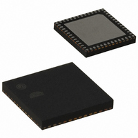
... Mechanical Details The EM250 package is a plastic 48-pin QFN that is 7mm x 7mm x 0.9mm. A large ground pad in the bottom center of the package forms a 49 PCB ground plane. For more information, refer to the EM250 Reference Design. Figure 17 illustrates the package drawing. Top View ...
Page 110
... EM250 9 Ordering Information Use the following part numbers to order the EM250: EM250-RTR Reel, RoHS EM250-RTY Tray, RoHS To order parts, contact Ember at +1-617-951-0200, or send your inquiry by email to sales@ember.com. Details about our international distributors can be found on our Web site: www.ember.com. 110 120-0082-000I ...
Page 111
... Register Address Table Table 40 provides the address, reset value, and description of the registers in the EM250. These registers are accessible by the application (user). Block: SERIAL Address Name 4400 SC2_RXBEGA 4402 SC2_RXENDA 4404 SC2_RXBEGB 4406 SC2_RXENDB 4408 SC2_TXBEGA 440A SC2_TXENDA 440C SC2_TXBEGB 440E ...
Page 112
... EM250 4492 SC1_RXCNTB 4494 SC1_TXCNT 4496 SC1_DMASTAT 4498 SC1_DMACTRL 449A SC1_RXERRA 449C SC1_RXERRB 449E SC1_DATA 44A0 SC1_SPISTAT 44A2 SC1_I2CSTAT 44A4 SC1_UARTSTAT 44A6 SC1_I2CCTRL1 44A8 SC1_I2CCTRL2 44AA SC1_MODE 44AC SC1_SPICFG 44AE SC1_UARTCFG 44B0 SC1_RATELIN 44B2 SC1_RATEEXP 44B4 SC1_UARTPER 44B6 SC1_UARTFRAC Block: TIMER1 ...
Page 113
... Interrupt config 0000 SC1 Interrupt config 0000 SC2 Interrupt config 0000 GPIO Interrupt config 0000 Timer Interrupt config 0000 GPIO Interrupt A config 0000 GPIO Interrupt B config 0000 GPIO Interrupt C config 0000 GPIO Interrupt D config 0000 Software interrupt EM250 120-0082-000I 113 ...
Page 114
... EM250 Block: GPIO Address Name 4700 GPIO_INH 4702 GPIO_INL 4704 GPIO_OUTH 4706 GPIO_OUTL 4708 GPIO_SETH 470A GPIO_SETL 470C GPIO_CLRH 470E GPIO_CLRL 4710 GPIO_DBG 4712 GPIO_CFG 4714 GPIO_DIRH 4716 GPIO_DIRL 4718 GPIO_DIRSETH 471A GPIO_DIRSETL 471C GPIO_DIRCLRH 471E GPIO_DIRCLRL 4720 GPIO_PDH 4722 GPIO_PDL ...
Page 115
... Low Noise Amplifier Link Quality Indicator Medium Access Control Moisture Sensitivity Level Mega samples per second Offset-Quadrature Phase Shift Keying Power Amplifier Packet Error Rate Physical Layer Phase-Locked Loop Power-On-Reset Power Spectral Density Power Supply Rejection Ratio Packet Trace Interface EM250 120-0082-000I 115 ...
Page 116
... EM250 Acronym/Abbreviation PWM RoHS RSSI SFD SIF SPI UART VCO VDD 116 120-0082-000I Meaning Pulse Width Modulation Restriction of Hazardous Substances Receive Signal Strength Indicator Start Frame Delimiter Serial Interface Serial Peripheral Interface Universal Asynchronous Receiver/Transmitter Voltage Controlled Oscillator Voltage Supply ...
Page 117
... ZigBee Specification v1.1 (www.zigbee.org; Document Number 053474r07) 5. ZigBee Security Services Specification v1.0 (Document Number 03322r13) 6. Ember EM250 Reference Design (www.ember.com) © 2005–2006 Ember Corporation. All rights reserved. The information in this document is subject to change without notice. This document is believed to be accu- rate and reliable, but the statements contained herein are presented without express or implied warranty ...