EM250-RTR Ember, EM250-RTR Datasheet - Page 27
EM250-RTR
Manufacturer Part Number
EM250-RTR
Description
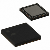
IC ZIGBEE SYSTEM-ON-CHIP 48-QFN
Manufacturer
Ember
Series
EM250r
Datasheet
1.EM250-JMP-R.pdf
(117 pages)
Specifications of EM250-RTR
Frequency
2.4GHz
Modulation Or Protocol
802.15.4 Zigbee
Applications
Home/Building Automation, Industrial Control and Monitoring
Power - Output
3dBm
Sensitivity
-97dBm
Voltage - Supply
2 V ~ 3.6 V
Current - Receiving
35.5mA
Current - Transmitting
33mA
Data Interface
PCB, Surface Mount
Memory Size
128kB Flash, 5kB SRAM
Antenna Connector
PCB, Surface Mount
Operating Temperature
-40°C ~ 85°C
Package / Case
48-QFN
For Use With
636-1009 - PROGRAMMER USB FLASH EM250/260
Lead Free Status / RoHS Status
Lead free / RoHS Compliant
Data Rate - Maximum
-
Other names
636-1000-2
Available stocks
Company
Part Number
Manufacturer
Quantity
Price
Company:

Part Number:
EM250-RTR
Manufacturer:
TI
Quantity:
3 400
Part Number:
EM250-RTR
Manufacturer:
EMBER
Quantity:
20 000


5 Functional Description—Application Modules
5.1
GPIO
In Application Mode, access to privileged areas are blocked while access to application-specific modules such
as GPIO, Serial Controllers (SC1 and SC2), General Purpose Timers, ADC, and Event Manager are enabled.
The EM250 has 17 multi-purpose GPIO pins that can be configured in a variety of ways. All pins have the fol-
lowing programmable features:
The information flow between the GPIO pin and its source are controlled by separate GPIO Data registers. The
GPIO_INH
registers enable the output signals for the GPIO Pins. The
resistors while
and
Instead of changing the entire contents to the
be applied. Writing to the
to 1, while data bits that are already 1 are maintained. Writing to the
ister changes individual register bits from 1 to 0, while data bits that are already 0 are maintained.
Note that the value read from
current pin state. To observe the pin state, the
All registers controlling the GPIO pin definitions are unaffected by power cycling the main core voltage
(VDD_CORE).
The
ing for alternate GPIO functions as listed in Table 17. Refer to Table 1 for individual pin alternate functions.
GPIO_OUTL
Selectable as input, output, or bi-directional.
Output can be totem pole, used as open drain or open source output for wired-OR applications.
Can have internal pull-up or pull-down.
GPIO_DBG
and
GPIO_INL
GPIO_PDH
register must always remain set to zero. The
control the output level.
Note (1) :
Note (2) :
GPIO_CFG
GPIO_PDH/L
registers report the input level of the GPIO pins. The
and
GPIO_PUH/L
GPIO_DIRSETH/L
GPIO_DIRH/L
GPIO_DIRCLRH/L
GPIO_SETH/L
GPIO_OUTH/L
GPIO_CLRH/L
GPIO_INH/L
GPIO_SETH/L
GPIO_PDL
GPIO_OUTH/L
Pull-down resistor is always disabled for Alternate GPIO functions
VREF_OUT, PTI_EN and PTI_DATA.
Pull-up resistor is always disabled for Alternate GPIO functions ADC 0,
ADC1, ADC2, ADC3, VREF_OUT, PTI_EN and PTI_DATA.
Figure 5. GPIO Control Logic
registers enable pull-down resistors on the GPIO Pins. The
or
GPIO_DIRSETH/L
,
GPIO_SETH/L
OUT/DIR
GPIO_INH/L
Alternate
functions
GPIO
registers with one write access, a limited change can
GPIO_PUH
VDD_PADS
, and
GPIO_CFG
registers should be read.
register changes individual register bits from 0
Note (1)
Note (2)
GPIO_CLRH/L
and
GPIO_CLRH/L
register controls the GPIO signal rout-
GPIO_PUL
GPIO[16:0]
GPIO_DIRH
registers may not reflect the
registers enable pull-up
or
GPIO_DIRCLRH/L
120-0082-000I
and
GPIO_DIRL
EM250
GPIO_OUTH
reg-
27
Related parts for EM250-RTR
Image
Part Number
Description
Manufacturer
Datasheet
Request
R

Part Number:
Description:
EM250 RCM BOARD
Manufacturer:
Ember
Datasheet:

Part Number:
Description:
EM250 BREAKOUT BOARD
Manufacturer:
Ember
Datasheet:

Part Number:
Description:
KIT JUMP START FOR EM250
Manufacturer:
Ember
Datasheet:

Part Number:
Description:
KIT EVAL EM250 RF TEST
Manufacturer:
Ember
Datasheet:

Part Number:
Description:
KIT DEV FOR EM250
Manufacturer:
Ember
Datasheet:

Part Number:
Description:
KIT DEV EMBER ZIGBEE W/PCWH
Manufacturer:
Custom Computer Services Inc (CCS)

Part Number:
Description:
PROGRAMMER USB FLASH EM250/260
Manufacturer:
Ember
Datasheet:

Part Number:
Description:
IC ZIGBEE SYSTEM-ON-CHIP 40-QFN
Manufacturer:
Ember
Datasheet:

Part Number:
Description:
IC RF TXRX ZIGBEE 128KB 48QFN
Manufacturer:
Ember
Datasheet:
Part Number:
Description:
IC RF TXRX ZIGBEE 192KB 48QFN
Manufacturer:
Ember
Datasheet:

Part Number:
Description:
INSIGHT ADAPTER FOR EM2XX
Manufacturer:
Ember
Datasheet:
Part Number:
Description:
PROGRAMMER USB FLASH EM250/260
Manufacturer:
Ember
Datasheet:
Part Number:
Description:
IC ZIGBEE SYSTEM-ON-CHIP 40-QFN
Manufacturer:
Ember
Datasheet:
Part Number:
Description:
IC RF TXRX ZIGBEE 128KB 48QFN
Manufacturer:
Ember
Datasheet:
Part Number:
Description:
IC RF TXRX ZIGBEE 192KB 48QFN
Manufacturer:
Ember
Datasheet: