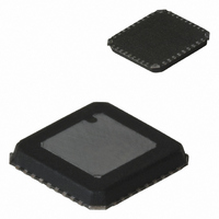
TB32301AFL Toshiba, TB32301AFL Datasheet

TB32301AFL
Specifications of TB32301AFL
Related parts for TB32301AFL
TB32301AFL Summary of contents
Page 1
... IF-IN1 RX2 RX3 AF2 FM-DET Tuning RSSI ×2 VCO1 PLL1 LOOP GND GND GND CC Syn2 FIL1 Syn2 Syn3 Syn1 1 TB32301AFL Weight: 0.08 g (typ.) Marking: TB32301AFL V CC RX2 AF1 D-DATA RSSI RX LPF 17 FLLC1 16 V RX2 CC V RX2 15 CC FLLC2 Filter TXIN 12 STB ...
Page 2
... Power supply pin CC 10 DATA Serial data input pin 11 CLK Serial clock input pin 12 STB Serial strobe input pin 13 TXIN Transmit signal input pin Function 3 2 TB32301AFL Equivalent Circuit V syn CC VCO GNDsyn 500 Ω 7 GND2 8 100 kΩ ...
Page 3
... FLLC1 16 V RX2 Power supply pin CC This pin drives out DC voltage according to the 18 RSSI RF input signal level. 19 DDATA Comparator output pin 20 AF1 Demodulation signal output pin Function 3 TB32301AFL Equivalent Circuit 1 kΩ FLL detector 18 500 Ω Dec./5 /2002 ...
Page 4
... Ground pin 24 GNDRX1 25 IFIN1 IF amplifier input pin 26 IFIN2 27 GNDRF3 Ground pin 28 MIXOUT1 Mixer output pin 29 MIXFIL Mixer filter pin 30 VCCRF1 Power supply pin 31 RFIN RF signal input pin Function 22 4 TB32301AFL Equivalent Circuit 450 Ω µA th Dec./5 /2002 ...
Page 5
... RF2 Power supply pin RF3 Power supply pin CC Note: The equivalent circuit diagrams above are intended as an aid for designing external circuits. They do not show the exact layout of the internal circuits. Function 5 TB32301AFL Equivalent Circuit th Dec./5 /2002 ...
Page 6
... Tuning (FLL), RX-AMP, RX-LPF, DATA COMP, FM-DET GND RX2 24 TX-FILTER, PA, RSSI, IF-AMP, (IF-BPF) GND RF1 32 LNA GND RF2 33 GND RX1 27 GND RF1 32 PA GND RF2 33 GND RX1 27 GND RF1 32 PA, MIXER, LNA GND RF2 33 Syn2 (2 pin) CC RFRX (30 pin TB32301AFL Block Name th Dec./5 /2002 ...
Page 7
... Functions and Operation 1. Serial data input timing chart • Data to control the TB32301AFL is serially applied to pins CLK, DATA and STB. • Data is loaded into shift registers with MSB first on the rising edge of the clock and latched on the rising edge of the STB signal. When the STB pin is high, the data stored in the shift register is retained even if clock is applied. When the STB pin is low, the data can be rewritten. • ...
Page 8
... Auto-tuning reference counter setting • The TB32301AFL has an automatic tuning system to correct the fluctuation of center frequency in FM detector, which is caused by, for example, temperature change. To generate a reference clock to correct the fluctuation, set the divide factor of auto-tuning reference counter to the value to obtain 200-kHz frequency, according to external reference clock frequency. • ...
Page 9
... Transmit power amplifier setting Applying data serially to pins CLK, DATA and STB changes the gain of the transmit power amplifier. The power control counter consists of 5 bits. MSB Group code (Control step number × Power control counter × --------- + P4 × TB32301AFL Dec./5 /2002 0 0 ...
Page 10
... Group code Note: Please clear the bits. • PLL charge pump current setting (CP1 and CP2 bits: 2.4 GHz) The TB32301AFL contains a constant current charge pump circuit. The output current of the circuit can be selected by setting the CP1 and CP2 bits. CP2 ...
Page 11
... Image canceller mixer in reception block The TB32301AFL contains an image canceller mixer as the first stage of the reception block. The image canceller mixer is designed for upper local, therefore, please set the local signal frequency to f0 (desired reception frequency MHz (IF frequency). 4. Lock detector function The TB32301AFL incorporates VCO lock detector function ...
Page 12
... VIH - CLK, DATA, STB, BS, TXIN VIL - CLK, DATA, STB, BS, TXIN Test Symbol Test Condition Circuit VIN(min) 1 S/N = 20dB Vin (LNA) = 70dBµV Vod - 12 TB32301AFL Unit °C Rating Unit 2.7 to 3.3 - °C Min Typ. Max Unit 28.0 35.1 42.0 ...
Page 13
... Vcp = 1/2V Icp ( Vcp = 1/2V Icp ( LD-off-LEAK 1 Open-drain output R(LD-on) 1 Open-drain output f (VCO - pn1 - @500 kHz pn2 @2 MHz - 13 TB32301AFL Ω 470 2400 2500 MHz 85 dBµV 0.36 0.54 0.72 V (1.25) (1 ...
Page 14
... 2450 MHz, Bit Rate = 100kHz, CC Vtx - SPRlo 1 Test frequency: 1.225 GHz dev (tx loop, fBB=100kHz (CW) PA-OUT 1 DATA21 set for PA output (nom.) PA-OUT 1 DATA3 set for PA output (min.) Z-OUT (PA TB32301AFL × V CC 0.8 0.2 −30 −20 dBm (140) (190) (230) KHz (−9) (− ...
Page 15
... Tuning (FLL) RSSI ×2 VCO1 PLL1 RFTX RF V LOOP GND GND GND CC Syn2 FIL1 Syn2 Syn3 Syn1 530 kHz T 15 TB32301AFL V (min) VOD IN V BER R201 1 kΩ R191 10 kΩ AF1 D-DATA CC RX2 18 C181 RSSI 1000 LPF C171 0.01 µ F ...
Page 16
... Package Dimensions Weight: 0.08 g (typ.) 16 TB32301AFL th Dec./5 /2002 ...
Page 17
... TOSHIBA CORPORATION for any infringements of intellectual property or other rights of the third parties which may result from its use. No license is granted by implication or otherwise under any intellectual property or other rights of TOSHIBA CORPORATION or othe • The information contained herein is subject to change without notice. rs. 17 TB32301AFL 000707EBA th Dec./5 /2002 ...


