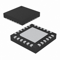
ATA8742-PXQW Atmel, ATA8742-PXQW Datasheet - Page 155

ATA8742-PXQW
Manufacturer Part Number
ATA8742-PXQW
Description
MCU W/TRANSMITTER ASK/FSK 24QFN
Manufacturer
Atmel
Datasheet
1.ATA8742-PXQW.pdf
(238 pages)
Specifications of ATA8742-PXQW
Frequency
433MHz
Applications
Home Automation, Remote Sensing, RKE
Modulation Or Protocol
ASK, FSK
Data Rate - Maximum
32 kBit/s
Power - Output
7.5dBm
Current - Transmitting
9.8mA
Data Interface
PCB, Surface Mount
Antenna Connector
PCB, Surface Mount
Memory Size
4kB Flash, 256B EEPROM, 256B SRAM
Voltage - Supply
2 V ~ 4 V
Operating Temperature
-40°C ~ 85°C
Package / Case
24-VQFN Exposed Pad, 24-HVQFN, 24-SQFN, 24-DHVQFN
Processor Series
ATA8x
Core
AVR8
Data Bus Width
8 bit
Program Memory Type
Flash
Program Memory Size
4 KB
Data Ram Size
256 B
Interface Type
SPI, USI
Maximum Clock Frequency
8.1 MHz
Number Of Programmable I/os
12
Number Of Timers
2
Maximum Operating Temperature
+ 85 C
Mounting Style
SMD/SMT
Development Tools By Supplier
ATASTK512-EK1-IND
Minimum Operating Temperature
- 40 C
On-chip Adc
10 bit, 8 Channel
Lead Free Status / RoHS Status
Lead free / RoHS Compliant
Features
-
Lead Free Status / Rohs Status
Details
Available stocks
Company
Part Number
Manufacturer
Quantity
Price
Company:
Part Number:
ATA8742-PXQW
Manufacturer:
ATMEL
Quantity:
1 482
- Current page: 155 of 238
- Download datasheet (4Mb)
25.3
9151A–INDCO–07/09
ADC Operation
Figure 25-1. Analog to Digital Converter Block Schematic
The ADC converts an analog input voltage to a 10-bit digital value through successive approxi-
mation. The minimum value represents GND and the maximum value represents the reference
voltage.The voltage reference for the ADC may be selected by writing to the REFS1..0 bits in
ADMUX. The VCC supply, the AREF pin or an internal 1.1V voltage reference may be selected
as the ADC voltage reference.
The analog input channel and differential gain are selected by writing to the MUX5..0 bits in
ADMUX. Any of the eight ADC input pins ADC7..0 can be selected as single ended inputs to the
ADC. For differential measurements all analog inputs next to each other can be selected as a
input pair. Every input is also possible to measure with ADC3. These pairs of differential inputs
are measured by ADC trough the differential gain amplifier.
If differential channels are selected, the differential gain stage amplifies the voltage difference
between the selected input pair by the selected gain factor, 1x or 20x, according to the setting of
ADC7
ADC6
ADC5
ADC4
ADC3
ADC2
ADC1
ADC0
AREF
V
CC
TEMPERATURE
REFERENCE
INTERNAL
8-BIT DATA BUS
AGND
ADC CTRL. & STATUS B
SENSOR
REGISTER (ADCSRB)
1.1V
ADC8
INPUT
INPUT
POS.
NEG.
MUX
ADTS2...ADTS0
MUX
ADC MULTIPLEXER
MUX DECODER
SELECT (ADMUX)
+
-
GAIN
AMPLIFIER
SINGLE ENDED / DIFFERENTIAL SELECTION
10-BIT DAC
ADC CTRL. & STATUS A
REGISTER (ADCSRA)
ADC CONVERSION
COMPLETE IRQ
PRESCALER
CONVERSION LOGIC
INTERRUPT
TRIGGER
SELECT
FLAGS
SAMPLE & HOLD
COMPARATOR
15
+
-
ADC DATA REGISTER
(ADCH/ADCL)
ADC MULTIPLEXER
OUTPUT
ATA8742
0
155
Related parts for ATA8742-PXQW
Image
Part Number
Description
Manufacturer
Datasheet
Request
R

Part Number:
Description:
Manufacturer:
ATMEL Corporation
Datasheet:

Part Number:
Description:
DEV KIT FOR AVR/AVR32
Manufacturer:
Atmel
Datasheet:

Part Number:
Description:
INTERVAL AND WIPE/WASH WIPER CONTROL IC WITH DELAY
Manufacturer:
ATMEL Corporation
Datasheet:

Part Number:
Description:
Low-Voltage Voice-Switched IC for Hands-Free Operation
Manufacturer:
ATMEL Corporation
Datasheet:

Part Number:
Description:
MONOLITHIC INTEGRATED FEATUREPHONE CIRCUIT
Manufacturer:
ATMEL Corporation
Datasheet:

Part Number:
Description:
AM-FM Receiver IC U4255BM-M
Manufacturer:
ATMEL Corporation
Datasheet:

Part Number:
Description:
Monolithic Integrated Feature Phone Circuit
Manufacturer:
ATMEL Corporation
Datasheet:

Part Number:
Description:
Multistandard Video-IF and Quasi Parallel Sound Processing
Manufacturer:
ATMEL Corporation
Datasheet:

Part Number:
Description:
High-performance EE PLD
Manufacturer:
ATMEL Corporation
Datasheet:

Part Number:
Description:
8-bit Flash Microcontroller
Manufacturer:
ATMEL Corporation
Datasheet:

Part Number:
Description:
2-Wire Serial EEPROM
Manufacturer:
ATMEL Corporation
Datasheet:


