STE48NM50 STMicroelectronics, STE48NM50 Datasheet
STE48NM50
Specifications of STE48NM50
Available stocks


Related parts for STE48NM50


STE48NM50 Summary of contents
Page 1
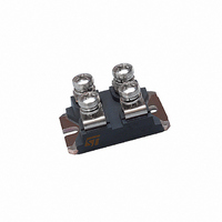
... Table 2: Order Codes SALES TYPE STE48NM50 March 2005 Figure 1: Package R I DS(on) D < 0 Figure 2: Internal Schematic Diagram product has an MARKING PACKAGE E48NM50 ISOTOP STE48NM50 MDmesh™ MOSFET ISOTOP PACKAGING TUBE Rev. 2 1/9 ...
Page 2
... STE48NM50 Table 3: Absolute Maximum ratings Symbol V Gate- source Voltage GS I Drain Current (continuous Drain Current (continuous Drain Current (pulsed Total Dissipation at T TOT Derating Factor dv/dt (*) Peak Diode Recovery voltage slope V Insulation Winthstand Voltage (AC-RMS) ISO T Storage Temperature stg T Max. Operating Junction Temperature ...
Page 3
... 4 (see Figure 14 400V 10V GS (see Figure 18) Test Conditions di/dt = 100 A/µ 100 25° (see Figure 16 di/dt = 100 A/µ 100 150° (see Figure 16) STE48NM50 Min. Typ. Max. Unit 20 S 3700 pF 610 1 117 Min. Typ. Max. Unit 48 A 192 A 1.5 V 520 ns 7.8 µ ...
Page 4
... STE48NM50 Figure 3: Safe Operating Area Figure 4: Output Characteristics Figure 5: Transconductance 4/9 Figure 6: Thermal Impedance Figure 7: Transfer Characteristics Figure 8: Static Drain-source On Resistance ...
Page 5
... Figure 9: Gate Charge vs Gate-source Voltage Figure 10: Normalized Gate Thereshold Volt- age vs Temperature Figure 11: Source-Drain Diode Forward Char- acteristics Figure 12: Capacitance Variations Figure 13: Normalized On Resistance vs Tem- perature STE48NM50 5/9 ...
Page 6
... STE48NM50 Figure 14: Unclamped Inductive Load Test Cir- cuit Figure 15: Switching Times Test Circuit For Resistive Load Figure 16: Test Circuit For Inductive Load Switching and Diode Recovery Times 6/9 Figure 17: Unclamped Inductive Wafeform Figure 18: Gate Charge Test Circuit ...
Page 7
... STE48NM50 MAX. 0.480 0.358 0.080 0.033 0.503 1.003 1.248 0.169 0.594 1.193 1.503 0.322 7/9 ...
Page 8
... STE48NM50 Table 9: Revision History Date Revision 30/Mar/2005 2 8/9 Description of Changes Modified value in table 7 ...
Page 9
... Australia - Belgium - Brazil - Canada - China - Czech Republic - Finland - France - Germany - Hong Kong - India - Israel - Italy - Japan - Malaysia - Malta - Morocco - Singapore - Spain - Sweden - Switzerland - United Kingdom - United States of America All other names are the property of their respective owners © 2005 STMicroelectronics - All Rights Reserved STMicroelectronics group of companies STE48NM50 9/9 ...