STE48NM50 STMicroelectronics, STE48NM50 Datasheet - Page 3
STE48NM50
Manufacturer Part Number
STE48NM50
Description
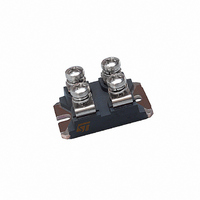
MOSFET N-CH 550V 48A ISOTOP
Manufacturer
STMicroelectronics
Series
MDmesh™r
Datasheet
1.STE48NM50.pdf
(9 pages)
Specifications of STE48NM50
Fet Type
MOSFET N-Channel, Metal Oxide
Fet Feature
Standard
Rds On (max) @ Id, Vgs
100 mOhm @ 24A, 10V
Drain To Source Voltage (vdss)
550V
Current - Continuous Drain (id) @ 25° C
48A
Vgs(th) (max) @ Id
5V @ 250µA
Gate Charge (qg) @ Vgs
117nC @ 10V
Input Capacitance (ciss) @ Vds
3700pF @ 25V
Power - Max
450W
Mounting Type
Chassis Mount
Package / Case
ISOTOP
Configuration
Single Dual Source
Transistor Polarity
N-Channel
Resistance Drain-source Rds (on)
0.1 Ohms
Forward Transconductance Gfs (max / Min)
20 S
Drain-source Breakdown Voltage
550 V
Gate-source Breakdown Voltage
+/- 30 V
Continuous Drain Current
48 A
Power Dissipation
450 W
Maximum Operating Temperature
+ 150 C
Mounting Style
Through Hole
Minimum Operating Temperature
- 65 C
Continuous Drain Current Id
24A
Drain Source Voltage Vds
550V
On Resistance Rds(on)
80mohm
Rds(on) Test Voltage Vgs
30V
Threshold Voltage Vgs Typ
4V
Rohs Compliant
Yes
Lead Free Status / RoHS Status
Lead free / RoHS Compliant
Other names
497-3170-5
Available stocks
Company
Part Number
Manufacturer
Quantity
Price

Part Number:
STE48NM50
Quantity:
213


ELECTRICAL CHARACTERISTICS (CONTINUED)
Table 7: Dynamic
Table 8: Source Drain Diode
Note: 1. Pulsed: Pulse duration = 300 µs, duty cycle 1.5 %.
Symbol
Symbol
I
V
SDM
g
t
t
C
SD
C
C
Q
d(on)
d(off)
Q
fs
I
I
R
I
2. Pulse width limited by safe operating area.
Q
Q
Q
rrm
rrm
SD
t
t
t
oss
t
t
iss
rss
rr
rr
c
gs
gd
r
f
(1)
G
g
rr
rr
(1)
(2)
Forward Transconductance
Input Capacitance
Output Capacitance
Reverse Transfer
Capacitance
Gate Input Resistance
Turn-on Delay Time
Rise Time
Turn-off Delay Time
Fall Time
Cross-over Time
Total Gate Charge
Gate-Source Charge
Gate-Drain Charge
Source-drain Current
Source-drain Current (pulsed)
Forward On Voltage
Reverse Recovery Time
Reverse Recovery Charge
Reverse Recovery Current
Reverse Recovery Time
Reverse Recovery Charge
Reverse Recovery Current
Parameter
Parameter
V
V
f=1 MHz Gate DC Bias = 0
Test Signal Level = 20mV
Open Drain
V
R
(see Figure 14)
V
V
(see Figure 18)
I
I
V
(see Figure 16)
I
V
(see Figure 16)
SD
SD
SD
DS
DS
DD
DD
GS
DD
DD
G
= 4.7
= 48 A, V
= 40 A, di/dt = 100 A/µs,
= 40 A, di/dt = 100 A/µs,
> I
= 25V, f = 1 MHz, V
= 250V, I
= 400V, I
= 10V
= 100 V, T
= 100 V, T
D(on)
Test Conditions
Test Conditions
V
x R
GS
GS
D
D
j
j
= 48 A,
DS(on)max,
= 10 V
= 25°C
= 150°C
= 24 A
= 0
GS
I
D
= 0
= 24A
Min.
Min.
3700
Typ.
Typ.
11.2
610
520
680
1.7
7.8
20
80
40
35
18
23
44
87
23
42
30
33
STE48NM50
Max.
Max.
117
192
1.5
48
Unit
Unit
nC
nC
nC
pF
pF
pF
ns
ns
ns
ns
ns
µC
µC
S
ns
ns
A
A
V
A
A
3/9
Related parts for STE48NM50
Image
Part Number
Description
Manufacturer
Datasheet
Request
R

Part Number:
Description:
STMicroelectronics [RIPPLE-CARRY BINARY COUNTER/DIVIDERS]
Manufacturer:
STMicroelectronics
Datasheet:
Part Number:
Description:
STMicroelectronics [LIQUID-CRYSTAL DISPLAY DRIVERS]
Manufacturer:
STMicroelectronics
Datasheet:

Part Number:
Description:
BOARD EVAL FOR MEMS SENSORS
Manufacturer:
STMicroelectronics
Datasheet:
Part Number:
Description:
NPN TRANSISTOR POWER MODULE
Manufacturer:
STMicroelectronics
Datasheet:
Part Number:
Description:
TURBOSWITCH ULTRA-FAST HIGH VOLTAGE DIODE
Manufacturer:
STMicroelectronics
Datasheet:
Part Number:
Description:
Manufacturer:
STMicroelectronics
Datasheet:
Part Number:
Description:
DIODE / SCR MODULE
Manufacturer:
STMicroelectronics
Datasheet:
Part Number:
Description:
DIODE / SCR MODULE
Manufacturer:
STMicroelectronics
Datasheet:
Part Number:
Description:
Search -----> STE16N100
Manufacturer:
STMicroelectronics
Datasheet:
Part Number:
Description:
Search ---> STE53NA50
Manufacturer:
STMicroelectronics
Datasheet:
Part Number:
Description:
NPN Transistor Power Module
Manufacturer:
STMicroelectronics
Datasheet:
Part Number:
Description:
DIODE / SCR MODULE
Manufacturer:
STMicroelectronics
Datasheet: