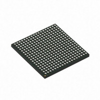
XC6SLX16-2CSG324C Xilinx Inc, XC6SLX16-2CSG324C Datasheet - Page 3
XC6SLX16-2CSG324C
Manufacturer Part Number
XC6SLX16-2CSG324C
Description
IC FPGA SPARTAN 6 14K 324CSGBGA
Manufacturer
Xilinx Inc
Series
Spartan® 6 LXr
Specifications of XC6SLX16-2CSG324C
Total Ram Bits
589824
Number Of Logic Elements/cells
14579
Number Of Labs/clbs
1139
Number Of I /o
232
Voltage - Supply
1.14 V ~ 1.26 V
Mounting Type
Surface Mount
Operating Temperature
0°C ~ 85°C
Package / Case
324-LFBGA, CSPBGA
No. Of Macrocells
14579
Family Type
Spartan-6
No. Of Speed Grades
2
No. Of I/o's
232
Clock Management
DCM, PLL
Core Supply Voltage Range
1.14V To
Lead Free Status / RoHS Status
Lead free / RoHS Compliant
Number Of Gates
-
Lead Free Status / RoHS Status
Lead free / RoHS Compliant, Lead free / RoHS Compliant
Other names
122-1671
Available stocks
Company
Part Number
Manufacturer
Quantity
Price
Company:

Part Number:
XC6SLX16-2CSG324C
Manufacturer:
XILINX44
Quantity:
1 260
Company:
Part Number:
XC6SLX16-2CSG324C
Manufacturer:
Xilinx Inc
Quantity:
10 000
Company:
Part Number:
XC6SLX16-2CSG324CES
Manufacturer:
Xilinx Inc
Quantity:
10 000


Table 2: Recommended Operating Conditions
Table 3: eFUSE Programming Conditions
DS162 (v2.0) March 31, 2011
Preliminary Product Specification
Notes:
1.
2.
3.
4.
5.
6.
7.
8.
9.
10. Do not exceed a total of 100 mA per bank.
11. V
Notes:
1.
2.
3.
R
Symbol
V
V
V
V
FUSE
Symbol
CCAUX
CCINT
BATT
FS
I
I
FS
IN
All voltages are relative to ground.
See Interface Performances for Memory Interfaces in
devices that do not support MCB functionality including the LX4 device, the TQG144 and CPG196 packages, and the -3N speed grade.
Recommended maximum voltage droop for V
During configuration, if V
The -1L devices require V
and PPDS_33 I/O standards on inputs. LVPECL_33 is not supported in the -1L devices.
Configuration data is retained even if V
Includes V
For PCI systems, the transmitter and receiver should have common supplies for V
Devices with a -1L speed grade do not support Xilinx PCI IP.
unconnected. When BBR is not used, Xilinx recommends connecting to V
t
These specifications apply during programming of the eFUSE AES key. Programming is only supported through JTAG.The AES key is only supported
in the following devices: XC6SLX75, XC6SLX75T, XC6SLX100, XC6SLX100T, XC6SLX150, and XC6SLX150T.
When programming eFUSE, V
connecting V
An R
connecting the R
j
BATT
(2)
(10)
(3)
(11)
FUSE
is required to maintain the battery backed RAM (BBR) AES key when V
External voltage supply
V
Auxiliary supply voltage relative to GND
External resistor from R
Internal supply voltage relative to GND
Temperature range
FS
resistor is required when programming the eFUSE AES key. When not programming or when eFUSE is not used, Xilinx recommends
CCO
Maximum current through pin using PCI
I/O standard when forward biasing the
clamp diode.
Battery voltage relative to GND, T
to +85C
(XC6SLX75, XC6SLX75T, XC6SLX100,
XC6SLX100T, XC6SLX150, and
XC6SLX150T only)
Battery voltage relative to GND,
T
XC6SLX75T, XC6SLX100,
XC6SLX100T, XC6SLX150, and
XC6SLX150T only)
supply current
j
FS
= –40C to +100C (XC6SLX75,
of 1.2V, 1.5V, 1.8V, 2.5V, and 3.3V.
to GND. However, V
FUSE
pin to V
CCO_2
Description
CCAUX
CCAUX
FS
is 1.8V, then
must be less than or equal to V
FUSE
= 2.5V when using the LVDS_25, LVDS_33, BLVDS_25, LVPECL_25, RSDS_25, RSDS_33, PPDS_25,
FS
or GND. However, R
CCO
can be between GND and 3.45 V.
pin to GND
drops to 0V.
V
CCAUX
CCAUX
j
= 0C
(1)
is 10 mV/ms.
Description
must be 2.5V.
Table
(1)
FUSE
Temperature
25. The standard V
Commercial
Commercial
(Cont’d)
Industrial
Industrial
www.xilinx.com
Range
can be unconnected.
Spartan-6 FPGA Data Sheet: DC and Switching Characteristics
CCAUX
. When not programming or when eFUSE is not used, Xilinx recommends
CCAUX
-3, -3N, -2,
-3, -3N, -2,
-3, -3N, -2,
-3, -3N,-2,
CCAUX
Speed
Grade
CCINT
-1L
-1L
-1L
-1L
or GND. However, V
CCO
(9)
(9)
is not applied. Once V
voltage range applies to designs not using an MCB, or to
.
Performance
Controller
Memory
Block
N/A
N/A
N/A
N/A
(2)
BATT
can be unconnected.
CCAUX
Min
1.0
–
–
is applied, V
1129
1.14
Min
3.2
3.2
15
–
Typ
–
–
–
1140
Typ
3.3
3.3
1.2
–
–
BATT
can be
Max
1151
3.6
Max
3.45
1.26
10
10
3.4
40
85
Units
Units
mA
mA
mA
°C
V
V
V
V
3
Related parts for XC6SLX16-2CSG324C
Image
Part Number
Description
Manufacturer
Datasheet
Request
R

Part Number:
Description:
FPGA, SPARTAN-6 LX, 14K, 324CSGBGA
Manufacturer:
Xilinx Inc
Datasheet:

Part Number:
Description:
FPGA, SPARTAN-6 LX, 14K, 256FTGBGA
Manufacturer:
Xilinx Inc
Datasheet:

Part Number:
Description:
FPGA, SPARTAN-6 LX, 14K, 256FTGBGA
Manufacturer:
Xilinx Inc
Datasheet:
Part Number:
Description:
FPGA Spartan®-6 Family 14579 Cells 45nm (CMOS) Technology 1.2V 256-Pin FTBGA
Manufacturer:
Xilinx Inc
Datasheet:
Part Number:
Description:
IC FPGA SPARTAN 6 14K 196CPGBGA
Manufacturer:
Xilinx Inc
Datasheet:
Part Number:
Description:
IC FPGA SPARTAN 6 14K 196CPGBGA
Manufacturer:
Xilinx Inc
Part Number:
Description:
IC FPGA SPARTAN 6 14K 196CPGBGA
Manufacturer:
Xilinx Inc
Datasheet:

Part Number:
Description:
IC FPGA SPARTAN 6 14K 225CSGBGA
Manufacturer:
Xilinx Inc
Datasheet:
Part Number:
Description:
IC FPGA SPARTAN 6 14K 256FTGBGA
Manufacturer:
Xilinx Inc
Datasheet:
Part Number:
Description:
IC FPGA SPARTAN 6 14K 225CSGBGA
Manufacturer:
Xilinx Inc
Datasheet:
Part Number:
Description:
IC FPGA SPARTAN 6 14K 225CSGBGA
Manufacturer:
Xilinx Inc
Datasheet:
Part Number:
Description:
IC FPGA SPARTAN 6 14K 256FTGBGA
Manufacturer:
Xilinx Inc
Datasheet:
Part Number:
Description:
IC FPGA SPARTAN 6 14K 196CPGBGA
Manufacturer:
Xilinx Inc
Datasheet:
Part Number:
Description:
IC FPGA SPARTAN 6 14K 196CPGBGA
Manufacturer:
Xilinx Inc
Datasheet:
Part Number:
Description:
IC FPGA SPARTAN 6 14K 225CSGBGA
Manufacturer:
Xilinx Inc
Datasheet: