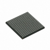
XC6SLX16-2CSG324C Xilinx Inc, XC6SLX16-2CSG324C Datasheet - Page 54

XC6SLX16-2CSG324C
Manufacturer Part Number
XC6SLX16-2CSG324C
Description
IC FPGA SPARTAN 6 14K 324CSGBGA
Manufacturer
Xilinx Inc
Series
Spartan® 6 LXr
Specifications of XC6SLX16-2CSG324C
Total Ram Bits
589824
Number Of Logic Elements/cells
14579
Number Of Labs/clbs
1139
Number Of I /o
232
Voltage - Supply
1.14 V ~ 1.26 V
Mounting Type
Surface Mount
Operating Temperature
0°C ~ 85°C
Package / Case
324-LFBGA, CSPBGA
No. Of Macrocells
14579
Family Type
Spartan-6
No. Of Speed Grades
2
No. Of I/o's
232
Clock Management
DCM, PLL
Core Supply Voltage Range
1.14V To
Lead Free Status / RoHS Status
Lead free / RoHS Compliant
Number Of Gates
-
Lead Free Status / RoHS Status
Lead free / RoHS Compliant, Lead free / RoHS Compliant
Other names
122-1671
Available stocks
Company
Part Number
Manufacturer
Quantity
Price
Company:
Part Number:
XC6SLX16-2CSG324C
Manufacturer:
XILINX44
Quantity:
1 260
Company:
Part Number:
XC6SLX16-2CSG324C
Manufacturer:
Xilinx Inc
Quantity:
10 000
Company:
Part Number:
XC6SLX16-2CSG324CES
Manufacturer:
Xilinx Inc
Quantity:
10 000
Table 55: Switching Characteristics for the Digital Frequency Synthesizer DFS (DCM_CLKGEN)
DS162 (v2.0) March 31, 2011
Preliminary Product Specification
Output Frequency Ranges (DCM_CLKGEN)
CLKOUT_FREQ_FX
CLKOUT_FREQ_FXDV
Output Clock Jitter
CLKOUT_PER_JITT_FX
CLKOUT_PER_JITT_FXDV Period jitter at the CLKFXDV
CLKFX_FREEZE_VAR
CLKFX_FREEZE_TEMP
_SLOPE
Duty Cycle
CLKOUT_DUTY_CYCLE_
FX
CLKOUT_DUTY_CYCLE_
FXDV
Lock Time
LOCK_FX
Symbol
(2)
(4)(5)
(2)(3)
Frequency for the CLKFX and
CLKFX180 outputs
Frequency for the CLKFXDV
output
Period jitter at the CLKFX and
CLKFX180 outputs.
output.
CLKFX period change in free
running oscillator mode at the
same temperature.
FCLKFX > 50 MHz
CLKFX period change in free
running oscillator mode at the
same temperature.
FCLKFX < 50 MHz
CLKFX period will change in
free_oscillator mode over
temperature. Add to
CLKFX_FREEZE_VAR to
determine total CLKFX period
change. Percentage change for
CLKFX period over 1°C.
Duty cycle precision for the
CLKFX and CLKFX180 outputs,
including the BUFGMUX and
clock tree duty-cycle distortion
Duty cycle precision for the
CLKFXDV outputs, including the
BUFGMUX and clock tree
duty-cycle distortion
The time from deassertion at the
DCM’s Reset input to the rising
transition at its LOCKED output.
The DFS asserts LOCKED when
the CLKFX, CLKFX180, and
CLKFXDV signals are valid.
Lock time requires
CLKFX_DIVIDE < F
MHz)
when:
5 MHz < F
when:
F
CLKIN
> 50 MHz
Description
CLKIN
< 50 MHz
IN
/(0.50
www.xilinx.com
Spartan-6 FPGA Data Sheet: DC and Switching Characteristics
0.15625
Min
5
–
–
-3
187.5
Max
375
50
Maximum = ±[1% of CLKFX period + 350]
Maximum = ±[1% of CLKFX period + 350]
5
Typical = ±[0.2% of CLKFX period + 100]
Typical = ±[0.2% of CLKFX period + 100]
Maximum = ±3% of CLKFX period
Maximum = ±5% of CLKFX period
0.15625
Min
5
–
–
-3N
Maximum = 0.1
Speed Grade
187.5
Max
375
50
5
0.15625
Min
5
–
–
-2
166.5
Max
333
50
5
0.15625
(1)
Min
5
–
–
-1L
Max
200
100
50
5
Units
%/°C
MHz
MHz
ms
ms
ps
ps
ps
ps
ps
ps
54


