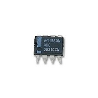
ADC0831 Parallax Inc, ADC0831 Datasheet - Page 14

ADC0831
Manufacturer Part Number
ADC0831
Description
ADC (A/D Converters) 8-bit ADC DIP ADC0831
Manufacturer
Parallax Inc
Datasheet
1.ADC0838CIWM.pdf
(32 pages)
Specifications of ADC0831
Lead Free Status / RoHS Status
Lead free / RoHS Compliant
Available stocks
Company
Part Number
Manufacturer
Quantity
Price
Company:
Part Number:
ADC0831
Manufacturer:
Parallax
Quantity:
135
Company:
Part Number:
ADC0831
Manufacturer:
TOS
Quantity:
5 510
Company:
Part Number:
ADC0831ACP
Manufacturer:
TI
Quantity:
5 510
Company:
Part Number:
ADC0831ACP
Manufacturer:
MOT
Quantity:
5 510
Part Number:
ADC0831CCN
Manufacturer:
NS/国半
Quantity:
20 000
Part Number:
ADC0831CCWM
Manufacturer:
NS/国半
Quantity:
20 000
www.national.com
Functional Description
Since the input configuration is under software control, it can
be modified, as required, at each conversion. A channel can
be treated as a single-ended, ground referenced input for
one conversion; then it can be reconfigured as part of a dif-
ferential channel for another conversion. Figure 1 illustrates
the input flexibility which can be achieved.
The analog input voltages for each channel can range from
50 mV below ground to 50 mV above V
out degrading conversion accuracy.
2.0 THE DIGITAL INTERFACE
A most important characteristic of these converters is their
serial data link with the controlling processor. Using a serial
communication format offers two very significant system im-
provements; it allows more function to be included in the
CC
(Continued)
(typically 5V) with-
TABLE 6. MUX Addressing: ADC0832
TABLE 7. MUX Addressing: ADC0832
COM is internally tied to A GND
Single-Ended MUX Mode
Differential MUX Mode
MUX Address
SGL/
MUX Address
SGL/
DIF
DIF
1
1
0
0
ODD/
SIGN
ODD/
SIGN
0
1
0
1
14
0
+
0
+
−
converter package with no increase in package size and it
can eliminate the transmission of low level analog signals by
locating the converter right at the analog sensor; transmitting
highly noise immune digital data back to the host processor.
To understand the operation of these converters it is best to
refer to the Timing Diagrams and Functional Block Diagram
and to follow a complete conversion sequence. For clarity a
separate diagram is shown of each device.
1. A conversion is initiated by first pulling the CS (chip select)
line low. This line must be held low for the entire conversion.
The converter is now waiting for a start bit and its MUX as-
signment word.
2. A clock is then generated by the processor (if not provided
continuously) and output to the A/D clock input.
Channel #
Channel #
1
+
1
−
+


