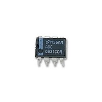
ADC0831 Parallax Inc, ADC0831 Datasheet - Page 15

ADC0831
Manufacturer Part Number
ADC0831
Description
ADC (A/D Converters) 8-bit ADC DIP ADC0831
Manufacturer
Parallax Inc
Datasheet
1.ADC0838CIWM.pdf
(32 pages)
Specifications of ADC0831
Lead Free Status / RoHS Status
Lead free / RoHS Compliant
Available stocks
Company
Part Number
Manufacturer
Quantity
Price
Company:
Part Number:
ADC0831
Manufacturer:
Parallax
Quantity:
135
Company:
Part Number:
ADC0831
Manufacturer:
TOS
Quantity:
5 510
Company:
Part Number:
ADC0831ACP
Manufacturer:
TI
Quantity:
5 510
Company:
Part Number:
ADC0831ACP
Manufacturer:
MOT
Quantity:
5 510
Part Number:
ADC0831CCN
Manufacturer:
NS/国半
Quantity:
20 000
Part Number:
ADC0831CCWM
Manufacturer:
NS/国半
Quantity:
20 000
Functional Description
3. On each rising edge of the clock the status of the data in
(DI) line is clocked into the MUX address shift register. The
start bit is the first logic “1” that appears on this line (all lead-
ing zeros are ignored). Following the start bit the converter
expects the next 2 to 4 bits to be the MUX assignment word.
4. When the start bit has been shifted into the start location
of the MUX register, the input channel has been assigned
and a conversion is about to begin. An interval of
riod (where nothing happens) is automatically inserted to al-
low the selected MUX channel to settle. The SAR status line
goes high at this time to signal that a conversion is now in
progress and the DI line is disabled (it no longer accepts
data).
5. The data out (DO) line now comes out of TRI-STATE and
provides a leading zero for this one clock period of MUX set-
tling time.
6. When the conversion begins, the output of the SAR com-
parator, which indicates whether the analog input is greater
than (high) or less than (low) each successive voltage from
the internal resistor ladder, appears at the DO line on each
falling edge of the clock. This data is the result of the conver-
sion being shifted out (with the MSB coming first) and can be
read by the processor immediately.
8 Single-Ended
4 Differential
FIGURE 1. Analog Input Multiplexer Options for the ADC0838
DS005583-53
DS005583-55
(Continued)
1
⁄
2
clock pe-
15
7. After 8 clock periods the conversion is completed. The
SAR status line returns low to indicate this
later.
8. If the programmer prefers, the data can be provided in an
LSB first format [this makes use of the shift enable (SE) con-
trol line]. All 8 bits of the result are stored in an output shift
register. On devices which do not include the SE control line,
the data, LSB first, is automatically shifted out the DO line,
after the MSB first data stream. The DO line then goes low
and stays low until CS is returned high. On the ADC0838 the
SE line is brought out and if held high, the value of the LSB
remains valid on the DO line. When SE is forced low, the
data is then clocked out LSB first. The ADC0831 is an excep-
tion in that its data is only output in MSB first format.
9. All internal registers are cleared when the CS line is high.
If another conversion is desired, CS must make a high to low
transition followed by address information.
The DI and DO lines can be tied together and controlled
through a bidirectional processor I/O bit with one wire. This is
possible because the DI input is only “looked-at” during the
MUX addressing interval while the DO line is still in a high
impedance state.
8 Pseudo-Differential
Mixed Mode
DS005583-56
DS005583-54
1
⁄
2
www.national.com
clock cycle


