ADC0831 Parallax Inc, ADC0831 Datasheet - Page 17
ADC0831
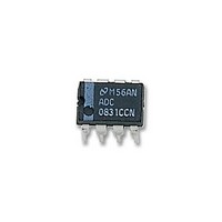
Manufacturer Part Number
ADC0831
Description
ADC (A/D Converters) 8-bit ADC DIP ADC0831
Manufacturer
Parallax Inc
Datasheet
1.ADC0838CIWM.pdf
(32 pages)
Specifications of ADC0831
Lead Free Status / RoHS Status
Lead free / RoHS Compliant
Available stocks
Company
Part Number
Manufacturer
Quantity
Price
Company:

Part Number:
ADC0831
Manufacturer:
Parallax
Quantity:
135
Company:
Part Number:
ADC0831
Manufacturer:
TOS
Quantity:
5 510
Company:
Part Number:
ADC0831ACP
Manufacturer:
TI
Quantity:
5 510
Company:
Part Number:
ADC0831ACP
Manufacturer:
MOT
Quantity:
5 510
Part Number:
ADC0831CCN
Manufacturer:
NS/国半
Quantity:
20 000
Part Number:
ADC0831CCWM
Manufacturer:
NS/国半
Quantity:
20 000


Functional Description
5.0 OPTIONAL ADJUSTMENTS
5.1 Zero Error
The zero of the A/D does not require adjustment. If the mini-
mum analog input voltage value, V
zero offset can be done. The converter can be made to out-
put 0000 0000 digital code for this minimum input voltage by
biasing any V
the differential mode operation of the A/D.
The zero error of the A/D converter relates to the location of
the first riser of the transfer function and can be measured by
grounding the V
positive voltage to the V
ence between the actual DC input voltage which is neces-
sary to just cause an output digital code transition from 0000
0000 to 0000 0001 and the ideal
mV for V
5.2 Full-Scale
The full-scale adjustment can be made by applying a differ-
ential input voltage which is 1
analog full-scale voltage range and then adjusting the mag-
nitude of the V
tal output code which is just changing from 1111 1110 to 1111
1111.
5.3 Adjusting for an Arbitrary Analog Input Voltage
Range
If the analog zero voltage of the A/D is shifted away from
ground (for example, to accommodate an analog input signal
which does not go to ground), this new zero reference
should be properly adjusted first. A V
equals this desired zero reference plus
LSB is calculated for the desired analog span, using 1 LSB =
analog span/256) is applied to selected “+” input and the
zero reference voltage at the corresponding “−” input should
then be adjusted to just obtain the 00
sition.
The full-scale adjustment should be made [with the proper
V
put which is given by:
where:
and
The V
change from FE
ment procedure.
6.0 POWER SUPPLY
A unique feature of the ADC0838 and ADC0834 is the inclu-
sion of a zener diode connected from the V
ground which also connects to the V
actual converter supply) through a silicon diode, as shown in
Figure 3 . (Note 3)
IN
(−) voltage applied] by forcing a voltage to the V
V
V
REF
MAX
MIN
REF
=
(or V
= the high end of the analog input range
= 5.000 V
IN
the low end (the offset zero) of the analog
range.
(Both are ground referenced.)
REF
CC
IN
(−) input at this V
HEX
) voltage is then adjusted to provide a code
(−) input and applying a small magnitude
input (or V
to FF
DC
).
IN
(+) input. Zero error is the differ-
HEX
CC
1
⁄
. This completes the adjust-
2
for the ADC0832) for a digi-
LSB down from the desired
1
IN(MIN)
⁄
2
CC
IN(MIN)
LSB value (
HEX
terminal (which is the
IN
(Continued)
to 01
1
value. This utilizes
⁄
(+) voltage which
2
, is not ground a
LSB (where the
HEX
+
1
⁄
terminal to
2
code tran-
LSB = 9.8
IN
(+) in-
17
This zener is intended for use as a shunt voltage regulator to
eliminate the need for any additional regulating components.
This is most desirable if the converter is to be remotely lo-
cated from the system power source. Figure 4 and Figure 5 il-
lustrate two useful applications of this on-board zener when
an external transistor can be afforded.
An important use of the interconnecting diode between V
and V
is used as a rectifier to allow the V
to be derived from the clock. The low current requirements of
the A/D and the relatively high clock frequencies used (typi-
cally in the range of 10k–400 kHz) allows using the small
value filter capacitor shown to keep the ripple on the V
to well under
also be used in this mode. This requires a clock voltage
swing which is in excess of V
needed, either built into the clock generator or a resistor can
be used from the CLK pin to the V
FIGURE 3. An On-Chip Shunt Regulator Diode
CC
is shown in Figure 6 and Figure 7 . Here, this diode
1
⁄
4
of an LSB. The shunt zener regulator can
Z
. A current limit for the zener is
CC
+
supply for the converter
pin.
DS005583-11
www.national.com
CC
line
+
Related parts for ADC0831
Image
Part Number
Description
Manufacturer
Datasheet
Request
R


Part Number:
Description:
Microcontroller Modules & Accessories DISCONTINUED BY PARALLAX
Manufacturer:
Parallax Inc

Part Number:
Description:
BOOK UNDERSTANDING SIGNALS
Manufacturer:
Parallax Inc
Datasheet:


Part Number:
Description:
COMPETITION RING FOR SUMOBOT
Manufacturer:
Parallax Inc
Datasheet:


Part Number:
Description:
TEXT INFRARED REMOTE FOR BOE-BOT
Manufacturer:
Parallax Inc
Datasheet:
Part Number:
Description:
BOARD EXPERIMENT+LCD NX-1000
Manufacturer:
Parallax Inc
Datasheet:

Part Number:
Description:
CONTROLLER 16SERVO MOTOR CONTROL
Manufacturer:
Parallax Inc
Datasheet:

Part Number:
Description:
BASIC STAMP LOGIC ANALYZER
Manufacturer:
Parallax Inc
Datasheet:

Part Number:
Description:
IC MCU 2K FLASH 50MHZ SO-18
Manufacturer:
Parallax Inc
Datasheet: