ADC0831 Parallax Inc, ADC0831 Datasheet - Page 5
ADC0831
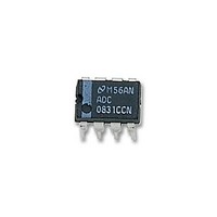
Manufacturer Part Number
ADC0831
Description
ADC (A/D Converters) 8-bit ADC DIP ADC0831
Manufacturer
Parallax Inc
Datasheet
1.ADC0838CIWM.pdf
(32 pages)
Specifications of ADC0831
Lead Free Status / RoHS Status
Lead free / RoHS Compliant
Available stocks
Company
Part Number
Manufacturer
Quantity
Price
Company:

Part Number:
ADC0831
Manufacturer:
Parallax
Quantity:
135
Company:
Part Number:
ADC0831
Manufacturer:
TOS
Quantity:
5 510
Company:
Part Number:
ADC0831ACP
Manufacturer:
TI
Quantity:
5 510
Company:
Part Number:
ADC0831ACP
Manufacturer:
MOT
Quantity:
5 510
Part Number:
ADC0831CCN
Manufacturer:
NS/国半
Quantity:
20 000
Part Number:
ADC0831CCWM
Manufacturer:
NS/国半
Quantity:
20 000


f
t
Clock Duty Cycle
(Note 10)
t
Data Input Valid to CLK
Rising Edge
t
after CLK Rising Edge
CONVERTER AND MULTIPLEXER CHARACTERISTICS
I
Current (Note 9)
DIGITAL AND DC CHARACTERISTICS
V
Voltage (Min)
V
Voltage (Max)
I
Current (Max)
I
Current (Max)
V
Voltage (Min)
V
Voltage (Max)
I
Current (Max)
I
Current (Min)
I
I
CLK
C
SET-UP
HOLD
ON
IN(1)
IN(0)
OUT
SOURCE
SINK
CC
The following specifications apply for V
Converter and Multiplexer Electrical Characteristics
V
apply from T
IN(1)
IN(0)
OUT(1)
OUT(0)
AC Characteristics
, Conversion Time
ADC0831, ADC0834,
ADC0838
ADC0832
, Supply Current (Max)
CC
, On Channel Leakage
, TRI-STATE Output
, Clock Frequency
, Logical “1” Input
, Logical “0” Input
, Output Sink Current (Min)
, Logical “1” Input
, Logical “0” Input
, Data Input Valid
= V+ = V
, Logical “1” Output
, Logical “0” Output
, Output Source
, CS Falling Edge or
Parameter
Parameter
MIN
REF
to T
= 5V, V
MAX
. (Continued)
REF
Min
Max
Min
Max
V
CC
On Channel = 0V,
Off Channel = 5V
On Channel = 5V,
Off Channel = 0V
V
V
V
V
V
I
I
V
I
V
V
V
V
Includes Ladder
Current
OUT
OUT
OUT
CC
CC
IN
IN
CC
CC
OUT
OUT
OUT
OUT
Conditions
+0.1V, T
= 5.0V
= 0V
= 5.25V
= 4.75V
= 4.75V
= 4.75V
= −360 µA
= −10 µA
= 1.6 mA
CC
= 0V
= 5V
= 0V
= V
Not including MUX Addressing Time
CC
= 5V, t
A
= T
r
= t
j
(Note 12)
Conditions
= 25˚C, and f
−0.005
f
0.005
−0.1
Typ
−14
0.1
0.9
2.3
= 20 ns and 25˚C unless otherwise specified.
16
CIWM Devices
(Note 13)
5
Tested
Limit
−0.2
+0.2
−6.5
CLK
2.0
0.8
2.4
4.5
0.4
8.0
2.5
6.5
−1
+1
−1
−3
1
3
= 250 kHz unless otherwise specified. Boldface limits
(Note 14)
Design
Limit
(Note 12)
Typ
(Note 12)
−0.005
The following specifications apply for
0.005
−0.1
Typ
−14
0.1
0.9
2.3
16
BCV, CCV, CCWM, BCN
and CCN Devices
(Note 13)
Tested
Limit
(Note 13)
10
Tested
8
Limit
−0.2
+0.2
−7.5
2.0
0.8
2.4
4.5
0.4
9.0
2.5
6.5
−1
−3
+3
1
(Note 14)
Design
(Note 14)
Limit
Design
400
250
Limit
−6.5
40
60
90
2.0
0.8
2.4
4.5
0.4
8.0
2.5
6.5
−1
+1
−1
−3
+3
1
www.national.com
1/f
Units
Units
Limit
mA
mA
mA
mA
kHz
kHz
µA
µA
µA
µA
µA
µA
ns
ns
V
V
V
V
V
%
%
CLK
Related parts for ADC0831
Image
Part Number
Description
Manufacturer
Datasheet
Request
R


Part Number:
Description:
Microcontroller Modules & Accessories DISCONTINUED BY PARALLAX
Manufacturer:
Parallax Inc

Part Number:
Description:
BOOK UNDERSTANDING SIGNALS
Manufacturer:
Parallax Inc
Datasheet:


Part Number:
Description:
COMPETITION RING FOR SUMOBOT
Manufacturer:
Parallax Inc
Datasheet:


Part Number:
Description:
TEXT INFRARED REMOTE FOR BOE-BOT
Manufacturer:
Parallax Inc
Datasheet:
Part Number:
Description:
BOARD EXPERIMENT+LCD NX-1000
Manufacturer:
Parallax Inc
Datasheet:

Part Number:
Description:
CONTROLLER 16SERVO MOTOR CONTROL
Manufacturer:
Parallax Inc
Datasheet:

Part Number:
Description:
BASIC STAMP LOGIC ANALYZER
Manufacturer:
Parallax Inc
Datasheet:

Part Number:
Description:
IC MCU 2K FLASH 50MHZ SO-18
Manufacturer:
Parallax Inc
Datasheet: