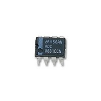
ADC0831 Parallax Inc, ADC0831 Datasheet - Page 16

ADC0831
Manufacturer Part Number
ADC0831
Description
ADC (A/D Converters) 8-bit ADC DIP ADC0831
Manufacturer
Parallax Inc
Datasheet
1.ADC0838CIWM.pdf
(32 pages)
Specifications of ADC0831
Lead Free Status / RoHS Status
Lead free / RoHS Compliant
Available stocks
Company
Part Number
Manufacturer
Quantity
Price
Company:
Part Number:
ADC0831
Manufacturer:
Parallax
Quantity:
135
Company:
Part Number:
ADC0831
Manufacturer:
TOS
Quantity:
5 510
Company:
Part Number:
ADC0831ACP
Manufacturer:
TI
Quantity:
5 510
Company:
Part Number:
ADC0831ACP
Manufacturer:
MOT
Quantity:
5 510
Part Number:
ADC0831CCN
Manufacturer:
NS/国半
Quantity:
20 000
Part Number:
ADC0831CCWM
Manufacturer:
NS/国半
Quantity:
20 000
www.national.com
Functional Description
3.0 REFERENCE CONSIDERATIONS
The voltage applied to the reference input to these convert-
ers defines the voltage span of the analog input (the differ-
ence between V
possible output codes apply. The devices can be used in ei-
ther ratiometric applications or in systems requiring absolute
accuracy. The reference pin must be connected to a voltage
source capable of driving the reference input resistance of
typically 3.5 k . This pin is the top of a resistor divider string
used for the successive approximation conversion.
In a ratiometric system, the analog input voltage is propor-
tional to the voltage used for the A/D reference. This voltage
is typically the system power supply, so the V
tied to V
relaxes the stability requirements of the system reference as
the analog input and A/D reference move together maintain-
ing the same output code for a given input condition.
4.0 THE ANALOG INPUTS
The most important feature of these converters is that they
can be located right at the analog signal source and through
just a few wires can communicate with a controlling proces-
sor with a highly noise immune serial bit stream. This in itself
greatly minimizes circuitry to maintain analog signal accu-
racy which otherwise is most susceptible to noise pickup.
However, a few words are in order with regard to the analog
inputs should the input be noisy to begin with or possibly
riding on a large common-mode voltage.
The differential input of these converters actually reduces
the effects of common-mode input noise, a signal common
to both selected “+” and “−” inputs for a conversion (60 Hz is
most typical). The time interval between sampling the “+” in-
put and then the “−” input is
in the common-mode voltage during this short time interval
can
common-mode signal this error is:
where f
cause
CM
CC
is the frequency of the common-mode signal,
(done internally on the ADC0832). This technique
conversion
IN(MAX)
a) Ratiometric
and V
1
⁄
2
errors.
of a clock period. The change
IN(MIN)
) over which the 256
For
(Continued)
DS005583-57
REF
a
FIGURE 2. Reference Examples
pin can be
sinusoidal
16
For absolute accuracy, where the analog input varies be-
tween very specific voltage limits, the reference pin can be
biased with a time and temperature stable voltage source.
The LM385 and LM336 reference diodes are good low cur-
rent devices to use with these converters.
The maximum value of the reference is limited to the V
supply voltage. The minimum value, however, can be quite
small (see Typical Performance Characteristics) to allow di-
rect conversions of transducer outputs providing less than a
5V output span. Particular care must be taken with regard to
noise pickup, circuit layout and system error voltage sources
when operating with a reduced span due to the increased
sensitivity of the converter (1 LSB equals V
For a 60 Hz common-mode signal to generate a
( 5 mV) with the converter running at 250 kHz, its peak value
would have to be 6.63V which would be larger than allowed
as it exceeds the maximum analog input limits.
Due to the sampling nature of the analog inputs short spikes
of current enter the “+” input and exit the “−” input at the
clock edges during the actual conversion. These currents
decay rapidly and do not cause errors as the internal com-
parator is strobed at the end of a clock period. Bypass ca-
pacitors at the inputs will average these currents and cause
an effective DC current to flow through the output resistance
of the analog signal source. Bypass capacitors should not be
used if the source resistance is greater than 1 k .
This source resistance limitation is important with regard to
the DC leakage currents of input multiplexer as well. The
worst-case leakage current of
create a 1 mV input error with a 1 k
op amp RC active low pass filter can provide both imped-
ance buffering and noise filtering should a high impedance
signal source be required.
V
and f
PEAK
b) Absolute with a reduced Span
CLK
is its peak voltage value
, is the A/D clock frequency.
±
1 µA over temperature will
source resistance. An
DS005583-58
REF
/256).
1
⁄
4
LSB error
CC


