ADC0831 Parallax Inc, ADC0831 Datasheet - Page 6
ADC0831
Manufacturer Part Number
ADC0831
Description
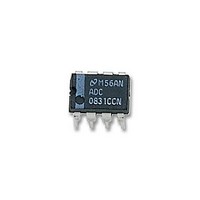
ADC (A/D Converters) 8-bit ADC DIP ADC0831
Manufacturer
Parallax Inc
Datasheet
1.ADC0838CIWM.pdf
(32 pages)
Specifications of ADC0831
Lead Free Status / RoHS Status
Lead free / RoHS Compliant
Available stocks
Company
Part Number
Manufacturer
Quantity
Price
Company:

Part Number:
ADC0831
Manufacturer:
Parallax
Quantity:
135
Company:
Part Number:
ADC0831
Manufacturer:
TOS
Quantity:
5 510
Company:
Part Number:
ADC0831ACP
Manufacturer:
TI
Quantity:
5 510
Company:
Part Number:
ADC0831ACP
Manufacturer:
MOT
Quantity:
5 510
Part Number:
ADC0831CCN
Manufacturer:
NS/国半
Quantity:
20 000
Part Number:
ADC0831CCWM
Manufacturer:
NS/国半
Quantity:
20 000


www.national.com
t
Edge to Output Data Valid
(Note 11)
t
CS to Data Output and
SARS Hi–Z
C
Input
C
Outputs
pd1
1H
The following specifications apply for V
AC Characteristics
IN
OUT
Note 1: Absolute Maximum Ratings indicate limits beyond which damage to the device may occur. DC and AC electrical specifications do not apply when operating
the device beyond its specified operating conditions.
Note 2: All voltages are measured with respect to the ground plugs.
Note 3: Internal zener diodes (6.3 to 8.5V) are connected from V+ to GND and V
to V
is powered from V+. Functionality is therefore guaranteed for V+ operation even though the resultant voltage at V
It is recommended that a resistor be used to limit the max current into V+. (See Figure 3 in Functional Description Section 6.0)
Note 4: When the input voltage (V
to 5 mA or less. The 20 mA package input current limits the number of pins that can exceed the power supply boundaries with a 5 mA current limit to four.
Note 5: Human body model, 100 pF discharged through a 1.5 k
Note 6: Total unadjusted error includes offset, full-scale, linearity, and multiplexer errors.
Note 7: Cannot be tested for ADC0832.
Note 8: For V
for analog input voltages one diode drop below ground or one diode drop greater than the V
level analog inputs (5V) can cause this input diode to conduct — especially at elevated temperatures, and cause errors for analog inputs near full-scale. The spec
allows 50 mV forward bias of either diode. This means that as long as the analog V
code will be correct. To achieve an absolute 0 V
tions, initial tolerance and loading.
Note 9: Leakage current is measured with the clock not switching.
Note 10: A 40% to 60% clock duty cycle range insures proper operation at all clock frequencies. In the case that an available clock has a duty cycle outside of these
limits, the minimum, time the clock is high or the minimum time the clock is low must be at least 1 µs. The maximum time the clock can be high is 60 µs. The clock
can be stopped when low so long as the analog input voltage remains stable.
Note 11: Since data, MSB first, is the output of the comparator used in the successive approximation loop, an additional delay is built in (see Block Diagram) to allow
for comparator response time.
Note 12: Typicals are at 25˚C and represent most likely parametric norm.
Note 13: Tested limits are guaranteed to National’s AOQL (Average Outgoing Quality Level).
Note 14: Guaranteed but not 100% production tested. These limits are not used to calculate outgoing quality levels.
Typical Performance Characteristics
Unadjusted Offset Error
vs V
, t
, Capacitance of Logic
, t
0H
CC
, Capacitance of Logic
pd0
REF
, — Rising Edge of
via a conventional diode. Since the zener voltage equals the A/D’s breakdown voltage, the diode insures that V
— CLK Falling
Voltage
IN
Parameter
(−) V
IN
(+) the digital output code will be 0000 0000. Two on-chip diodes are tied to each analog input (see Block Diagram) which will forward conduct
IN
) at any pin exceeds the power supply rails (V
DS005583-43
(Continued)
DC
CC
C
Data MSB First
Data LSB First
C
(see TRI-STATE
C
to 5 V
L
L
L
= 100 pF
= 10 pF, R
= 100 pf, R
= 5V, t
DC
Linearity Error vs V
Voltage
input voltage range will therefore require a minimum supply voltage of 4.950 V
r
= t
Conditions
L
L
resistor.
f
= 10k
= 2k
= 20 ns and 25˚C unless otherwise specified.
®
Test Circuits)
6
CC
IN
IN
REF
to GND. The zener at V+ can operate as a shunt regulator and is connected
<
or V
V
−
REF
or V
CC
DS005583-44
does not exceed the supply voltage by more than 50 mV, the output
IN
supply. Be careful, during testing at low V
>
V
(Note 12)
+
) the absolute value of current at that pin should be limited
Typ
650
250
125
5
5
CC
Linearity Error vs
Temperature
may exceed the specified Absolute Max of 6.5V.
CC
(Note 13)
will be below breakdown when the device
Tested
Limit
500
DC
(Note 14)
CC
Design
over temperature varia-
Limit
1500
levels (4.5V), as high
600
250
DS005583-45
Units
Limit
pF
pF
ns
ns
ns
ns
Related parts for ADC0831
Image
Part Number
Description
Manufacturer
Datasheet
Request
R


Part Number:
Description:
Microcontroller Modules & Accessories DISCONTINUED BY PARALLAX
Manufacturer:
Parallax Inc

Part Number:
Description:
BOOK UNDERSTANDING SIGNALS
Manufacturer:
Parallax Inc
Datasheet:


Part Number:
Description:
COMPETITION RING FOR SUMOBOT
Manufacturer:
Parallax Inc
Datasheet:


Part Number:
Description:
TEXT INFRARED REMOTE FOR BOE-BOT
Manufacturer:
Parallax Inc
Datasheet:
Part Number:
Description:
BOARD EXPERIMENT+LCD NX-1000
Manufacturer:
Parallax Inc
Datasheet:

Part Number:
Description:
CONTROLLER 16SERVO MOTOR CONTROL
Manufacturer:
Parallax Inc
Datasheet:

Part Number:
Description:
BASIC STAMP LOGIC ANALYZER
Manufacturer:
Parallax Inc
Datasheet:

Part Number:
Description:
IC MCU 2K FLASH 50MHZ SO-18
Manufacturer:
Parallax Inc
Datasheet: