SSM3K124TU(TE85L) Toshiba, SSM3K124TU(TE85L) Datasheet
SSM3K124TU(TE85L)
Manufacturer Part Number
SSM3K124TU(TE85L)
Description
MOSFET Small Signal Vds=30V Id=2.4A 3Pin
Manufacturer
Toshiba
Datasheet
1.SSM3K124TUTE85L.pdf
(5 pages)
Specifications of SSM3K124TU(TE85L)
Configuration
Single
Transistor Polarity
N-Channel
Resistance Drain-source Rds (on)
0.088 Ohms
Forward Transconductance Gfs (max / Min)
4.9 S / 2.5 S
Drain-source Breakdown Voltage
30 V
Continuous Drain Current
2.4 A
Power Dissipation
800 mW
Mounting Style
SMD/SMT
Package / Case
2-2U1A
Lead Free Status / RoHS Status
Lead free / RoHS Compliant


High Speed Switching Applications
•
•
•
Maximum Ratings
Electrical Characteristics
Note 1: Mounted on a ceramic board.
Note 2: Mounted on an FR4 board.
Note3: Pulse test
4 V drive
Low ON-resistance:
Lead(Pb)-free
Drain–source voltage
Gate–source voltage
Drain current
Drain power dissipation
Channel temperature
Storage temperature range
Drain–source breakdown voltage
Drain cutoff current
Gate leakage current
Gate threshold voltage
Forward transfer admittance
Drain–source ON-resistance
Input capacitance
Output capacitance
Reverse transfer capacitance
Switching time
Drain–source forward voltage
(25.4 mm × 25.4 mm × 0.8 t, Cu Pad: 645 mm
(25.4 mm × 25.4 mm × 1.6 t, Cu Pad: 645 mm
Characteristic
Characteristic
Turn-on time
Turn-off time
TOSHIBA Field Effect Transistor Silicon N Channel MOS Type
(Ta = 25°C)
DC
Pulse
R
R
on
on
= 120 mΩ (max) (@V
= 83 mΩ (max) (@V
(Ta = 25°C)
SSM3K124TU
V
P
P
R
Symbol
Symbol
(BR) DSS
⏐Y
D (Note 1)
D (Note 2)
DS (ON)
V
I
I
C
V
C
C
GSS
DSS
V
V
t
t
T
DSF
T
I
oss
on
off
GSS
rss
I
DP
iss
stg
th
fs
DS
D
ch
⏐
I
V
V
V
V
I
I
V
V
V
V
V
I
D
D
D
D
DS
GS
DS
DS
DS
DS
DS
DD
GS
GS
GS
= 1 mA, V
= 1.5 A, V
= 1.0 A, V
= − 2.4 A, V
= 30 V, V
= 5 V, I
= 5 V, I
= 10 V, V
= 10 V, V
= 10 V, V
−55~150
= ± 20 V, V
= 10 V, I
= 0 to 4 V, R
Rating
= 4V)
= 10V)
2
2
± 20
800
500
150
2.4
4.8
30
)
)
1
D
D
Test Condition
GS
GS
GS
D
GS
= 1 mA
= 1.5 A
GS
GS
GS
GS
= 1.5 A,
= 0
DS
= 10 V
= 4 V
G
= 0
= 0, f = 1 MHz
= 0, f = 1 MHz
= 0, f = 1 MHz
= 0 V
= 0
= 10 Ω
Unit
mW
°C
°C
V
V
A
(Note3)
(Note3)
(Note3)
(Note3)
Weight: 6.6 mg (typ.)
JEDEC
JEITA
TOSHIBA
UFM
Min
1.1
2.5
30
⎯
⎯
⎯
⎯
⎯
⎯
⎯
⎯
⎯
⎯
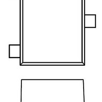
1 :Gate
2 :Source
3 :Drain
1
2
SSM3K124TU
– 0.9
Typ.
180
100
4.9
64
88
38
13
14
⎯
⎯
⎯
⎯
2.1±0.1
1.7±0.1
2-2U1A
2005-01-31
– 1.25
―
―
Max
120
2.6
±1
83
⎯
⎯
⎯
⎯
⎯
⎯
⎯
1
3
Unit: mm
Unit
mΩ
µA
µA
pF
pF
pF
ns
V
V
S
V
Related parts for SSM3K124TU(TE85L)
Image
Part Number
Description
Manufacturer
Datasheet
Request
R

Part Number:
Description:
High Speed Switching Applications
Manufacturer:
Toshiba Semiconductor
Datasheet:

Part Number:
Description:
Toshiba Semiconductor [TOSHIBA IGBT Module Silicon N Channel IGBT]
Manufacturer:
TOSHIBA Semiconductor CORPORATION
Datasheet:
Part Number:
Description:
TOSHIBA GTR MODULE SILICON NPN TRIPLE DIFFUSED TYPE
Manufacturer:
TOSHIBA Semiconductor CORPORATION
Datasheet:
Part Number:
Description:
TOSHIBA GTR Module Silicon N Channel IGBT
Manufacturer:
TOSHIBA Semiconductor CORPORATION
Datasheet:
Part Number:
Description:
TOSHIBA Intelligent Power Module Silicon N Channel IGBT
Manufacturer:
TOSHIBA Semiconductor CORPORATION
Datasheet:
Part Number:
Description:
TOSHIBA INTELLIGENT POWER MODULE SILICON N CHANNEL LGBT
Manufacturer:
TOSHIBA Semiconductor CORPORATION
Datasheet:
Part Number:
Description:
TOSHIBA IGBT Module Silicon N Channel IGBT
Manufacturer:
TOSHIBA Semiconductor CORPORATION
Datasheet:
Part Number:
Description:
TOSHIBA GTR MODULE SILICON N−CHANNEL IGBT
Manufacturer:
TOSHIBA Semiconductor CORPORATION
Datasheet:
Part Number:
Description:
TOSHIBA Intelligent Power Module Silicon N Channel IGBT
Manufacturer:
TOSHIBA Semiconductor CORPORATION
Datasheet:
Part Number:
Description:
TOSHIBA GTR Module Silicon N Channel IGBT
Manufacturer:
TOSHIBA Semiconductor CORPORATION
Datasheet:
Part Number:
Description:
TOSHIBA INTELLIGENT POWER MODULE
Manufacturer:
TOSHIBA Semiconductor CORPORATION
Datasheet:
Part Number:
Description:
TOSHIBA Intelligent Power Module Silicon N Channel IGBT
Manufacturer:
TOSHIBA Semiconductor CORPORATION
Datasheet:
Part Number:
Description:
TOSHIBA Intelligent Power Module Silicon N Channel IGBT
Manufacturer:
TOSHIBA Semiconductor CORPORATION
Datasheet:
Part Number:
Description:
TOSHIBA IGBT Module Silicon N Channel IGBT
Manufacturer:
TOSHIBA Semiconductor CORPORATION
Datasheet:
Part Number:
Description:
TOSHIBA Intelligent Power Module Silicon N Channel IGBT
Manufacturer:
TOSHIBA Semiconductor CORPORATION
Datasheet:
SSM3K124TU(TE85L) Summary of contents
Page 1
... TOSHIBA Field Effect Transistor Silicon N Channel MOS Type SSM3K124TU High Speed Switching Applications • drive • Low ON-resistance 120 mΩ (max) (@ mΩ (max) (@V on • Lead(Pb)-free Maximum Ratings (Ta = 25°C) Characteristic Drain–source voltage Gate–source voltage DC Drain current Pulse ...
Page 2
Switching Time Test Circuit (a) Test Circuit µ Ω D.U. < < Common Source ...
Page 3
I – 3.6V VGS = 3. Common Source Ta = 25° 0.4 0.6 0.8 0.2 Drain–source voltage V ( – (ON) ...
Page 4
Common Source 25° 0.3 0.1 1 0.01 0.1 Drain current I ( – 1000 500 300 C iss 100 C ...
Page 5
SSM3K124TU 5 2005-01-31 ...