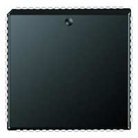
PIC18F6680-I/L Microchip Technology, PIC18F6680-I/L Datasheet - Page 169

PIC18F6680-I/L
Manufacturer Part Number
PIC18F6680-I/L
Description
Microcontrollers (MCU) 64KB 3328 RAM 52 I/O
Manufacturer
Microchip Technology
Datasheet
1.PCM18XK1.pdf
(496 pages)
Specifications of PIC18F6680-I/L
Processor Series
PIC18F
Core
PIC
Data Bus Width
8 bit
Data Ram Size
3.25 KB
Interface Type
I2C/SPI/AUSART/CAN
Maximum Clock Frequency
40 MHz
Number Of Programmable I/os
53
Number Of Timers
5
Operating Supply Voltage
4.2 V to 5.5 V
Maximum Operating Temperature
+ 85 C
Mounting Style
SMD/SMT
3rd Party Development Tools
52715-96, 52716-328, 52717-734, 52712-325, EWPIC18
Development Tools By Supplier
PG164130, DV164035, DV244005, DV164005, PG164120, ICE2000, ICE4000, DV164136
Minimum Operating Temperature
- 40 C
On-chip Adc
12-ch x 10-bit
Program Memory Type
Flash
Program Memory Size
64 KB
Package / Case
PLCC-68
Lead Free Status / RoHS Status
Lead free / RoHS Compliant
Available stocks
Company
Part Number
Manufacturer
Quantity
Price
Company:
Part Number:
PIC18F6680-I/L
Manufacturer:
RUBYCON
Quantity:
46 000
Part Number:
PIC18F6680-I/L
Manufacturer:
MICROCH
Quantity:
20 000
- Current page: 169 of 496
- Download datasheet (9Mb)
15.0
PIC18FXX80/XX85 devices contain a total of two CCP
modules: CCP1 and CCP2. CCP1 is an enhanced
version of the CCP2 module. CCP1 is fully backward
compatible with the CCP2 module.
The CCP1 module differs from CCP2 in the following
respect:
• CCP1 contains a special trigger event that may
• CCP1 contains “CAN Message Time-Stamp Trigger”
• CCP1 contains enhanced PWM output with
REGISTER 15-1:
2004 Microchip Technology Inc.
reset Timer1 or the Timer3 register pair
programmable dead band and auto-shutdown
functionality
CAPTURE/COMPARE/PWM
(CCP) MODULES
bit 7-6
bit 5-4
bit 3-0
CCP1CON REGISTER
bit 7
P1M1:P1M0: Enhanced PWM Output Configuration bits
If CCP1M<3:2> = 00, 01, 10:
xx =P1A assigned as capture/compare input; P1B, P1C, P1D assigned as port pins
If CCP1M<3:2> = 11:
00 = Single output; P1A modulated; P1B, P1C, P1D assigned as port pins
01 = Full-bridge output forward; P1D modulated; P1A active; P1B, P1C inactive
10 = Half-bridge output; P1A, P1B modulated with dead-band control; P1C, P1D assigned as
11 = Full-bridge output reverse; P1B modulated; P1C active; P1A, P1D inactive
DC1B1:DC1B0: PWM Duty Cycle bit 1 and bit 0
Capture mode:
Unused.
Compare mode:
Unused.
PWM mode:
These bits are the two LSbs of the 10-bit PWM duty cycle. The eight MSbs of the duty cycle are
found in CCPR1L.
CCP1M3:CCP1M0: Enhanced CCP Mode Select bits
0000 = Capture/Compare/PWM off (resets CCP1 module)
0001 = Reserved
0010 = Compare mode, toggle output on match
0011 = Reserved
0100 = Capture mode, every falling edge
0101 = Capture mode, every rising edge
0110 = Capture mode, every 4th rising edge
0111 = Capture mode, every 16th rising edge
1000 = Compare mode, initialize CCP pin low, on compare match force CCP pin high
1001 = Compare mode, initialize CCP pin high, on compare match force CCP pin low
1010 = Compare mode, generate software interrupt only, CCP pin is unaffected
1011 = Compare mode, trigger special event, resets TMR1 or TMR3
1100 = PWM mode; P1A, P1C active-high; P1B, P1D active-high
1101 = PWM mode; P1A, P1C active-high; P1B, P1D active-low
1110 = PWM mode; P1A, P1C active-low; P1B, P1D active-high
1111 = PWM mode; P1A, P1C active-low; P1B, P1D active-low
Legend:
R = Readable bit
- n = Value at POR
R/W-0
P1M1
port pins
R/W-0
P1M0
PIC18F6585/8585/6680/8680
DC1B1
R/W-0
W = Writable bit
‘1’ = Bit is set
DC1B0
R/W-0
Additionally, the CCP2 special event trigger may be
used to start an A/D conversion if the A/D module is
enabled.
To avoid duplicate information, this section describes
basic CCP module operation that applies to both CCP1
and CCP2. Enhanced CCP functionality of the
CCP1 module is described in Section 16.0 “Enhanced
Capture/Compare/PWM (ECCP) Module”.
The control registers for the CCP1 and CCP2 modules
are shown in Register 15-1 and Register 15-2,
respectively. Table 15-2 details the interactions of the
CCP and ECCP modules.
CCP1M3
U = Unimplemented bit, read as ‘0’
‘0’ = Bit is cleared
R/W-0
CCP1M2
R/W-0
x = Bit is unknown
CCP1M1
R/W-0
DS30491C-page 167
CCP1M0
R/W-0
bit 0
Related parts for PIC18F6680-I/L
Image
Part Number
Description
Manufacturer
Datasheet
Request
R

Part Number:
Description:
20-Pin USB Flash Microcontrollers
Manufacturer:
MICROCHIP [Microchip Technology]
Datasheet:

Part Number:
Description:
PIC18F With 128-segment LCD Driver And 12-bit ADC, 8KB Flash, 768B RAM, CCP, MSS
Manufacturer:
Microchip Technology
Datasheet:

Part Number:
Description:
PIC18F With 128-segment LCD Driver And 12-bit ADC, 16KB Flash, 768B RAM, CCP, MS
Manufacturer:
Microchip Technology
Datasheet:

Part Number:
Description:
PIC18F With 192-segment LCD Driver And 12-bit ADC, 8KB Flash, 768B RAM, CCP, MSS
Manufacturer:
Microchip Technology
Datasheet:

Part Number:
Description:
PIC18F With 192-segment LCD Driver And 12-bit ADC, 16KB Flash, 768B RAM, CCP, MS
Manufacturer:
Microchip Technology
Datasheet:

Part Number:
Description:
Microcontrollers (MCU) 48KB 3328 RAM 52 I/O
Manufacturer:
Microchip Technology
Datasheet:

Part Number:
Description:
32kB Flash, 2kB RAM, 1kB EE, NanoWatt XLP, LCD 64 QFN 9x9x0.9mm T/R
Manufacturer:
Microchip Technology
Datasheet:

Part Number:
Description:
32kB Flash, 2kB RAM, 1kB EE, NanoWatt XLP, LCD 64 TQFP 10x10x1mm T/R
Manufacturer:
Microchip Technology
Datasheet:

Part Number:
Description:
128kB Flash, 4kB RAM, 1kB EE, 16MIPS, NanoWatt XLP, LCD, 5V 80 TQFP 12x12x1mm T/
Manufacturer:
Microchip Technology
Datasheet:

Part Number:
Description:
32kB Flash, 2kB RAM, 1kB EE, NanoWatt XLP, LCD 64 QFN 9x9x0.9mm TUBE
Manufacturer:
Microchip Technology
Datasheet:

Part Number:
Description:
32kB Flash, 2kB RAM, 1kB EE, NanoWatt XLP, LCD 64 TQFP 10x10x1mm TRAY
Manufacturer:
Microchip Technology

Part Number:
Description:
128kB Flash, 4kB RAM, 1kB EE, 16MIPS, NanoWatt XLP, LCD, 5V 80 TQFP 12x12x1mm TR
Manufacturer:
Microchip Technology

Part Number:
Description:
Manufacturer:
Microchip Technology Inc.
Datasheet:


