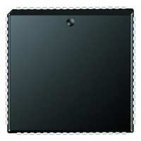
PIC18F6680-I/L Microchip Technology, PIC18F6680-I/L Datasheet - Page 449

PIC18F6680-I/L
Manufacturer Part Number
PIC18F6680-I/L
Description
Microcontrollers (MCU) 64KB 3328 RAM 52 I/O
Manufacturer
Microchip Technology
Datasheet
1.PCM18XK1.pdf
(496 pages)
Specifications of PIC18F6680-I/L
Processor Series
PIC18F
Core
PIC
Data Bus Width
8 bit
Data Ram Size
3.25 KB
Interface Type
I2C/SPI/AUSART/CAN
Maximum Clock Frequency
40 MHz
Number Of Programmable I/os
53
Number Of Timers
5
Operating Supply Voltage
4.2 V to 5.5 V
Maximum Operating Temperature
+ 85 C
Mounting Style
SMD/SMT
3rd Party Development Tools
52715-96, 52716-328, 52717-734, 52712-325, EWPIC18
Development Tools By Supplier
PG164130, DV164035, DV244005, DV164005, PG164120, ICE2000, ICE4000, DV164136
Minimum Operating Temperature
- 40 C
On-chip Adc
12-ch x 10-bit
Program Memory Type
Flash
Program Memory Size
64 KB
Package / Case
PLCC-68
Lead Free Status / RoHS Status
Lead free / RoHS Compliant
Available stocks
Company
Part Number
Manufacturer
Quantity
Price
Company:
Part Number:
PIC18F6680-I/L
Manufacturer:
RUBYCON
Quantity:
46 000
Part Number:
PIC18F6680-I/L
Manufacturer:
MICROCH
Quantity:
20 000
- Current page: 449 of 496
- Download datasheet (9Mb)
FIGURE 27-25:
TABLE 27-26: A/D CONVERSION REQUIREMENTS
2004 Microchip Technology Inc.
130
131
132
135
136
Note 1:
Param.
No.
Note 1: If the A/D clock source is selected as RC, a time of T
2:
3:
4:
5:
A/D DATA
SAMPLE
A/D CLK
ADRES
2: This is a minimal RC delay (typically 100 ns) which also disconnects the holding capacitor from the analog input.
T
T
T
T
T
Symbol
BSF ADCON0, GO
AD
CNV
ACQ
SWC
AMP
ADIF
ADRES register may be read on the following T
See Section 19.0 “10-bit Analog-to-Digital Converter (A/D) Module” for minimum conditions when input
voltage has changed more than 1 LSb.
The time for the holding capacitor to acquire the “New” input voltage when the voltage changes full scale
after the conversion (AV
50 .
On the next Q4 cycle of the device clock.
The time of the A/D clock period is dependent on the device frequency and the T
executed.
GO
Q4
132
A/D Clock Period
Conversion Time
(not including acquisition time) (Note 1)
Acquisition Time (Note 3)
Switching Time from Convert
Amplifier Settling Time (Note 2)
A/D CONVERSION TIMING
(Note 2)
Characteristic
DD
9
to AV
PIC18FXX8X
PIC18LFXX8X
PIC18FXX8X
PIC18LFXX8X
8
SS
PIC18F6585/8585/6680/8680
, or AV
OLD_DATA
7
Sample
CY
SS
is added before the A/D clock starts. This allows the SLEEP instruction to be
. . .
SAMPLING STOPPED
to AV
CY
DD
cycle.
. . .
131
130
). The source impedance (R
Min
1.6
3.0
2.0
3.0
11
15
10
—
1
2
(Note 4)
20
20
Max
6.0
9.0
12
—
—
—
(5)
(5)
1
Units
T
AD
s
s
s
s
s
s
s
0
T
T
A/D RC mode
A/D RC mode
-40 C
0 C
This may be used if the
“new” input voltage has not
changed by more than 1 LSb
(i.e., 5 mV @ 5.12V) from the
last sampled voltage (as
stated on C
OSC
OSC
AD
S
) on the input channels is
clock divider.
based, V
based, V
Temp
NEW_DATA
DONE
Temp
Conditions
DS30491C-page 447
HOLD
T
CY
+125 C
REF
REF
+125 C
).
full range
3.0V
Related parts for PIC18F6680-I/L
Image
Part Number
Description
Manufacturer
Datasheet
Request
R

Part Number:
Description:
20-Pin USB Flash Microcontrollers
Manufacturer:
MICROCHIP [Microchip Technology]
Datasheet:

Part Number:
Description:
PIC18F With 128-segment LCD Driver And 12-bit ADC, 8KB Flash, 768B RAM, CCP, MSS
Manufacturer:
Microchip Technology
Datasheet:

Part Number:
Description:
PIC18F With 128-segment LCD Driver And 12-bit ADC, 16KB Flash, 768B RAM, CCP, MS
Manufacturer:
Microchip Technology
Datasheet:

Part Number:
Description:
PIC18F With 192-segment LCD Driver And 12-bit ADC, 8KB Flash, 768B RAM, CCP, MSS
Manufacturer:
Microchip Technology
Datasheet:

Part Number:
Description:
PIC18F With 192-segment LCD Driver And 12-bit ADC, 16KB Flash, 768B RAM, CCP, MS
Manufacturer:
Microchip Technology
Datasheet:

Part Number:
Description:
Microcontrollers (MCU) 48KB 3328 RAM 52 I/O
Manufacturer:
Microchip Technology
Datasheet:

Part Number:
Description:
32kB Flash, 2kB RAM, 1kB EE, NanoWatt XLP, LCD 64 QFN 9x9x0.9mm T/R
Manufacturer:
Microchip Technology
Datasheet:

Part Number:
Description:
32kB Flash, 2kB RAM, 1kB EE, NanoWatt XLP, LCD 64 TQFP 10x10x1mm T/R
Manufacturer:
Microchip Technology
Datasheet:

Part Number:
Description:
128kB Flash, 4kB RAM, 1kB EE, 16MIPS, NanoWatt XLP, LCD, 5V 80 TQFP 12x12x1mm T/
Manufacturer:
Microchip Technology
Datasheet:

Part Number:
Description:
32kB Flash, 2kB RAM, 1kB EE, NanoWatt XLP, LCD 64 QFN 9x9x0.9mm TUBE
Manufacturer:
Microchip Technology
Datasheet:

Part Number:
Description:
32kB Flash, 2kB RAM, 1kB EE, NanoWatt XLP, LCD 64 TQFP 10x10x1mm TRAY
Manufacturer:
Microchip Technology

Part Number:
Description:
128kB Flash, 4kB RAM, 1kB EE, 16MIPS, NanoWatt XLP, LCD, 5V 80 TQFP 12x12x1mm TR
Manufacturer:
Microchip Technology

Part Number:
Description:
Manufacturer:
Microchip Technology Inc.
Datasheet:


