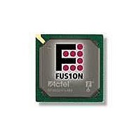
AFS600-PQG208 Actel, AFS600-PQG208 Datasheet - Page 184

AFS600-PQG208
Manufacturer Part Number
AFS600-PQG208
Description
FPGA - Field Programmable Gate Array 600K System Gates
Manufacturer
Actel
Datasheet
1.AFS600-PQG208.pdf
(330 pages)
Specifications of AFS600-PQG208
Processor Series
AFS600
Core
IP Core
Maximum Operating Frequency
1098.9 MHz
Number Of Programmable I/os
95
Data Ram Size
110592
Supply Voltage (max)
1.575 V
Maximum Operating Temperature
+ 70 C
Minimum Operating Temperature
0 C
Development Tools By Supplier
AFS-Eval-Kit, AFS-BRD600, FlashPro 3, FlashPro Lite, Silicon-Explorer II, Silicon-Sculptor 3, SI-EX-TCA
Mounting Style
SMD/SMT
Supply Voltage (min)
1.425 V
Number Of Gates
600 K
Package / Case
PQFP-208
Lead Free Status / RoHS Status
Lead free / RoHS Compliant
Available stocks
Company
Part Number
Manufacturer
Quantity
Price
Company:
Part Number:
AFS600-PQG208
Manufacturer:
Actel
Quantity:
135
Company:
Part Number:
AFS600-PQG208I
Manufacturer:
Microsemi SoC
Quantity:
10 000
- Current page: 184 of 330
- Download datasheet (13Mb)
Device Architecture
Table 2-87 • Summary of AC Measuring Points
Table 2-88 • I/O AC Parameter Definitions
2- 16 8
Standard
3.3 V LVTTL / 3.3 V LVCMOS
2.5 V LVCMOS
1.8 V LVCMOS
1.5 V LVCMOS
3.3 V PCI
3.3 V PCI-X
3.3 V GTL
2.5 V GTL
3.3 V GTL+
2.5 V GTL+
HSTL (I)
HSTL (II)
SSTL2 (I)
SSTL2 (II)
SSTL3 (I)
SSTL3 (II)
LVDS
LVPECL
Parameter
t
t
t
t
t
t
t
t
t
t
t
t
DP
PY
DOUT
EOUT
DIN
PYS
HZ
ZH
LZ
ZL
ZHS
ZLS
Applicable to All I/O Bank Types
Summary of I/O Timing Characteristics – Default I/O Software Settings
Data to Pad delay through the Output Buffer
Pad to Data delay through the Input Buffer with Schmitt trigger disabled
Data to Output Buffer delay through the I/O interface
Enable to Output Buffer Tristate Control delay through the I/O interface
Input Buffer to Data delay through the I/O interface
Pad to Data delay through the Input Buffer with Schmitt trigger enabled
Enable to Pad delay through the Output Buffer—High to Z
Enable to Pad delay through the Output Buffer—Z to High
Enable to Pad delay through the Output Buffer—Low to Z
Enable to Pad delay through the Output Buffer—Z to Low
Enable to Pad delay through the Output Buffer with delayed enable—Z to High
Enable to Pad delay through the Output Buffer with delayed enable—Z to Low
Input Reference Voltage
(V
REF_TYP
0.75 V
0.75 V
1.25 V
1.25 V
0.8 V
0.8 V
1.0 V
1.0 V
1.5 V
1.5 V
–
–
–
–
–
–
–
–
)
R e visio n 1
Definition
Board Termination Voltage
(V
1.485 V
1.485 V
0.75 V
0.75 V
1.25 V
1.25 V
TT_REF
1.2 V
1.2 V
1.5 V
1.5 V
–
–
–
–
–
–
–
–
)
Measuring Trip Point
0.615 * VCCI (FF))
0.285 * VCCI (RR)
0.285 * VCCI (RR)
0.615 * VCCI (FF)
Cross point
Cross point
(V
0.90 V
0.75 V
VREF
VREF
VREF
VREF
VREF
VREF
VREF
VREF
VREF
VREF
1.4 V
1.2 V
trip
)
Related parts for AFS600-PQG208
Image
Part Number
Description
Manufacturer
Datasheet
Request
R

Part Number:
Description:
AFS600-1FGG256I
Manufacturer:
Actel
Datasheet:

Part Number:
Description:
AFS600-2FGG256I
Manufacturer:
Actel
Datasheet:


