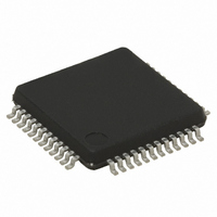
STM32F100C6T6BTR STMicroelectronics, STM32F100C6T6BTR Datasheet - Page 33

STM32F100C6T6BTR
Manufacturer Part Number
STM32F100C6T6BTR
Description
IC ARM CORTEX MCU 32KB 48LQFP
Manufacturer
STMicroelectronics
Series
STM32r
Datasheet
1.STM32F100R4T6B.pdf
(87 pages)
Specifications of STM32F100C6T6BTR
Core Processor
ARM® Cortex-M3™
Core Size
32-Bit
Speed
24MHz
Connectivity
I²C, IrDA, LIN, SPI, UART/USART
Peripherals
DMA, PDR, POR, PVD, PWM, Temp Sensor, WDT
Number Of I /o
37
Program Memory Size
32KB (32K x 8)
Program Memory Type
FLASH
Ram Size
4K x 8
Voltage - Supply (vcc/vdd)
2 V ~ 3.6 V
Data Converters
A/D 10x12b; D/A 2x12b
Oscillator Type
Internal
Operating Temperature
-40°C ~ 85°C
Package / Case
48-LFQFP
Core
ARM Cortex M3
For Use With
STM32100B-EVAL - EVAL BOARD FOR STM32F100VBT6
Lead Free Status / RoHS Status
Lead free / RoHS Compliant
Eeprom Size
-
Lead Free Status / Rohs Status
Details
Available stocks
Company
Part Number
Manufacturer
Quantity
Price
Company:
Part Number:
STM32F100C6T6BTR
Manufacturer:
STMicroelectronics
Quantity:
10 000
Part Number:
STM32F100C6T6BTR
Manufacturer:
ST
Quantity:
20 000
STM32F100x4, STM32F100x6, STM32F100x8, STM32F100xB
5.3
5.3.1
Table 6.
1. All main power (V
2. Negative injection disturbs the analog performance of the device.
3. Positive injection is not possible on these I/Os. A negative injection is induced by V
4.
5. When several inputs are submitted to a current injection, the maximum ΣI
Table 7.
Operating conditions
General operating conditions
Table 8.
Symbol
V
supply, in the permitted range.
never be exceeded. Refer to
values.
never be exceeded. Refer to
values.
positive and negative injected currents (instantaneous values).
f
f
I
A positive injection is induced by V
f
PCLK1
PCLK2
ΣI
V
DDA
INJ(PIN)
HCLK
Symbol
V
BAT
DD
INJ(PIN)
Symbol
I
I
VDD
VSS
I
T
IO
(1)
STG
T
J
(2)
Current characteristics
Thermal characteristics
General operating conditions
Internal AHB clock frequency
Internal APB1 clock frequency
Internal APB2 clock frequency
Standard operating voltage
Analog operating voltage
(ADC not used)
Analog operating voltage
(ADC used)
Backup operating voltage
Total current into V
Total current out of V
Output current sunk by any I/O and control pin
Output current source by any I/Os and control pin
Injected current on five volt tolerant pins
Injected current on any other pin
Total injected current (sum of all I/O and control pins)
DD
, V
Storage temperature range
Maximum junction temperature
DDA
Parameter
) and ground (V
Table 5: Voltage characteristics
Table 5: Voltage characteristics
Doc ID 16455 Rev 6
IN
>V
DD
DD
SS
/V
Ratings
SS
while a negative injection is induced by V
DDA
ground lines (sink)
, V
Ratings
SSA
Must be the same potential
as V
power lines (source)
) pins must always be connected to the external power
DD
(4)
Conditions
for the maximum allowed input voltage
for the maximum allowed input voltage
(3)
(1)
SeeNote: on page
(1)
INJ(PIN)
(5)
Electrical characteristics
–65 to +150
is the absolute sum of the
Min
IN
2.4
1.8
Value
IN
150
0
0
0
2
2
69.
<V
<V
SS
+5 / –0
SS
. I
Max.
± 25
150
150
−25
± 5
25
. I
INJ(PIN)
Max
3.6
3.6
3.6
3.6
24
24
24
INJ(PIN)
must
must
Unit
MHz
Unit
Unit
°C
°C
mA
V
V
V
33/87


