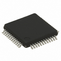
STM32F100C6T6BTR STMicroelectronics, STM32F100C6T6BTR Datasheet - Page 68

STM32F100C6T6BTR
Manufacturer Part Number
STM32F100C6T6BTR
Description
IC ARM CORTEX MCU 32KB 48LQFP
Manufacturer
STMicroelectronics
Series
STM32r
Datasheet
1.STM32F100R4T6B.pdf
(87 pages)
Specifications of STM32F100C6T6BTR
Core Processor
ARM® Cortex-M3™
Core Size
32-Bit
Speed
24MHz
Connectivity
I²C, IrDA, LIN, SPI, UART/USART
Peripherals
DMA, PDR, POR, PVD, PWM, Temp Sensor, WDT
Number Of I /o
37
Program Memory Size
32KB (32K x 8)
Program Memory Type
FLASH
Ram Size
4K x 8
Voltage - Supply (vcc/vdd)
2 V ~ 3.6 V
Data Converters
A/D 10x12b; D/A 2x12b
Oscillator Type
Internal
Operating Temperature
-40°C ~ 85°C
Package / Case
48-LFQFP
Core
ARM Cortex M3
For Use With
STM32100B-EVAL - EVAL BOARD FOR STM32F100VBT6
Lead Free Status / RoHS Status
Lead free / RoHS Compliant
Eeprom Size
-
Lead Free Status / Rohs Status
Details
Available stocks
Company
Part Number
Manufacturer
Quantity
Price
Company:
Part Number:
STM32F100C6T6BTR
Manufacturer:
STMicroelectronics
Quantity:
10 000
Part Number:
STM32F100C6T6BTR
Manufacturer:
ST
Quantity:
20 000
Electrical characteristics
Table 42.
1. Based on characterization results, not tested in production.
2. Guaranteed by design, not tested in production.
3. In devices delivered in LQFP packages, V
4. For external triggers, a delay of 1/f
68/87
t
Symbol
STAB
t
R
C
f
R
CONV
V
V
t
TRIG
I
t
V
CAL
t
f
ADC
ADC
VREF
f
latr
t
AIN
Devices that come in the TFBGA64 package have a V
see
AIN
lat
REF+
ADC
S
S
DDA
(2)
(2)
(2)
(2)
(2)
(2)
(3)
(2)
(2)
(2)
(2)
(2)
Table 4: STM32F100xx pin definitions
Power supply
Positive reference voltage
Current on the V
pin
ADC clock frequency
Sampling rate
External trigger frequency
Conversion voltage range
External input impedance
Sampling switch resistance
Internal sample and hold
capacitor
Calibration time
Injection trigger conversion
latency
Regular trigger conversion
latency
Sampling time
Power-up time
Total conversion time
(including sampling time)
ADC characteristics
Equation 1: R
R
AIN
Parameter
<
------------------------------------------------------------- - R
f
ADC
REF
×
AIN
input
C
PCLK2
ADC
max formula:
T
S
×
must be added to the latency specified in
REF+
ln
and
(
2
STM32F100x4, STM32F100x6, STM32F100x8, STM32F100xB
See
Table 43
is internally connected to V
Figure
N
f
f
f
f
f
f
+
ADC
ADC
ADC
ADC
ADC
ADC
Doc ID 16455 Rev 6
2
Conditions
Equation 1
)
REF+
–
6.
= 12 MHz
= 12 MHz
= 12 MHz
= 12 MHz
= 12 MHz
= 12 MHz
for details
ADC
pin but no V
and
REF-
14 to 252 (t
successive approximation)
DDA
0 (V
pin (V
and V
ground)
SSA
0.125
1.17
0.05
Min
2.4
2.4
0.6
1.5
REF-
Table
0
REF-
tied to
S
is internally connected to V
42.
for sampling +12.5 for
is internally connected to V
5.9
83
160
Typ
0
(1)
V
220
0.214
0.143
239.5
V
Max
17.1
823
3
2
3.6
REF+
12
17
50
21
DDA
1
1
8
1
(4)
(4)
(1)
SSA
SSA
1/f
1/f
1/f
1/f
1/f
1/f
),
MHz
MHz
Unit
kHz
µA
kΩ
kΩ
pF
µs
µs
µs
µs
µs
µs
V
V
ADC
V
ADC
ADC
ADC
ADC
ADC
.


