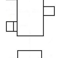
SSM3K7002FUT5LF Toshiba, SSM3K7002FUT5LF Datasheet

SSM3K7002FUT5LF
Specifications of SSM3K7002FUT5LF
Related parts for SSM3K7002FUT5LF
SSM3K7002FUT5LF Summary of contents
Page 1
... TOSHIBA Field Effect Transistor Silicon N Channel MOS Type SSM3K7002FU High Speed Switching Applications Analog Switch Applications • Small package • = 3.3 Ω (max) (@V Low ON resistance : 3.2 Ω (max) (@ 3.0 Ω (max) (@ Maximum Ratings (Ta = 25°C) Characteristics Drain-Source voltage Gate-Source voltage DC Drain current Pulse Drain power dissipation (Ta = 25° ...
Page 2
Electrical Characteristics (Ta = 25°C) Characteristics Gate leakage current Drain-Source breakdown voltage Drain cut-off current Gate threshold voltage Forward transfer admittance Drain-Source ON resistance Input capacitance Reverse transfer capacitance Output capacitance Turn-on delay time Switching time Turn-off delay time Switching ...
Page 3
ID - VDS 1000 Common Source 900 Ta=25°C 5 800 7 700 10 600 500 400 300 200 100 VGS=2. 0.5 1 1.5 Drain-Source voltage VDS (V) RDS(ON Common Source Ta=25° 5.0V VGS=4.5V ...
Page 4
ID 1000 100 Common source VDS=10V Ta=25° 100 Drain current ID (mA VDS 100 Common Source VGS=0V f=1MHz Ta=25°C Ciss 10 Coss Crss 1 0 Drain-Source voltage VDS ( ...
Page 5
... TOSHIBA is continually working to improve the quality and reliability of its products. Nevertheless, semiconductor devices in general can malfunction or fail due to their inherent electrical sensitivity and vulnerability to physical stress the responsibility of the buyer, when utilizing TOSHIBA products, to comply with the standards of safety in making a safe design for the entire system, and to avoid situations in which a malfunction or failure of such TOSHIBA products could cause loss of human life, bodily injury or damage to property ...


