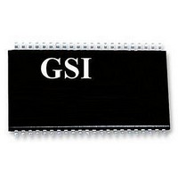
GS74108AGP-10I GSI TECHNOLOGY, GS74108AGP-10I Datasheet

GS74108AGP-10I
Specifications of GS74108AGP-10I
Related parts for GS74108AGP-10I
GS74108AGP-10I Summary of contents
Page 1
... V power supply *All GSI Technology packages are at least 5/6 RoHS compliant. Packages listed with the additional “G” designator are 6/6 RoHS compliant. Rev: 1.07 1/2006 Specifications cited are subject to change without notice. For latest documentation see http://www.gsitechnology.com. 512K x 8 ...
Page 2
Rev: 1.07 1/2006 Specifications cited are subject to change without notice. For latest documentation see http://www.gsitechnology.com. TSOP-II 512K x 8-Pin Configuration ...
Page 3
Truth Table Note: X: “H” or “L” Absolute Maximum Ratings Parameter Supply Voltage Input Voltage Output Voltage Allowable power dissipation Storage temperature Note: Permanent device ...
Page 4
Capacitance Parameter Symbol Input Capacitance C IN Output Capacitance C OUT Notes: 1. Tested 25° MHz A 2. These parameters are sampled and are not 100% tested. DC I/O Pin Characteristics Parameter Symbol Input ...
Page 5
AC Test Conditions Parameter Input high level Input low level Input rise time Input fall time Input reference level Output reference level Output load Notes: 1. Include scope and jig capacitance. 2. Test conditions as specified with output loading as ...
Page 6
Address Data Out Address CE OE Data Out Rev: 1.07 1/2006 Specifications cited are subject to change without notice. For latest documentation see http://www.gsitechnology.com. Read Cycle ...
Page 7
Write Cycle Parameter Write cycle time Address valid to end of write Chip enable to end of write Data set up time Data hold time Write pulse width Address set up time Write recovery time (WE) Write recovery time (CE) ...
Page 8
Address Data In Data Out Rev: 1.07 1/2006 Specifications cited are subject to change without notice. For latest documentation see http://www.gsitechnology.com. Write Cycle 2: CE control ...
Page 9
Rev: 1.07 1/2006 Specifications cited are subject to change without notice. For latest documentation see http://www.gsitechnology.com. 44-Pin, 400 mil TSOP- Symbol ...
Page 10
Pin A1 Index A A1 Pin Index Rev: 1.07 1/2006 Specifications cited are subject to change without notice. For latest documentation see http://www.gsitechnology.com ...
Page 11
... GS74108ATP-8I GS74108ATP-10I GS74108ATP-12I GS74108AGP-8 RoHS-compliant 400 mil TSOP-II GS74108AGP-10 RoHS-compliant 400 mil TSOP-II GS74108AGP-12 RoHS-compliant 400 mil TSOP-II GS74108AGP-8I RoHS-compliant 400 mil TSOP-II GS74108AGP-10I RoHS-compliant 400 mil TSOP-II GS74108AGP-12I RoHS-compliant 400 mil TSOP-II GS74108AJ-8 GS74108AJ-10 GS74108AJ-12 GS74108AJ-8I GS74108AJ-10I GS74108AJ-12I GS74108AGJ-8 RoHS-compliant 400 mil SOJ ...
Page 12
... Customers requiring delivery in Tape and Reel should add the character “T” to the end of the part number. For example: GS74108ATP-8T. 2. All GSI Technology packages are at least 5/6 RoHS compliant. Packages listed with the additional “G” designator are 6/6 RoHS compliant. 3. ...
Page 13
Asynchronous Datasheet Revision History Rev. Code: Old; Types of Changes New Format or Content 74108A_r1 74108A_r1; 74108A_r1_01 74108A_r1_01; 74108A_r1_02 74108A_r1_02; 74108A_r1_03 74108A_r1_03; 74108A_r1_04 74108A_r1_04; 74108A_r1_05 74108A_r1_05; 74108A_r1_06 74108A_r1_06; 74108A_r1_07 Rev: 1.07 1/2006 Specifications cited are subject to change without ...


