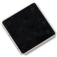
LPC2468FBD208 NXP Semiconductors, LPC2468FBD208 Datasheet - Page 64

LPC2468FBD208
Manufacturer Part Number
LPC2468FBD208
Description
IC, 32BIT MCU, ARM7, 72MHZ, LQFP-208
Manufacturer
NXP Semiconductors
Datasheet
1.LPC2468FBD208.pdf
(85 pages)
Specifications of LPC2468FBD208
Controller Family/series
(ARM7)
No. Of I/o's
160
Ram Memory Size
98KB
Cpu Speed
72MHz
No. Of Timers
4
No. Of Pwm Channels
12
Core Size
32 Bit
Program Memory Size
512KB
Rohs Compliant
Yes
Oscillator Type
External, Internal
Lead Free Status / RoHS Status
Lead free / RoHS Compliant
Available stocks
Company
Part Number
Manufacturer
Quantity
Price
Company:
Part Number:
LPC2468FBD208
Manufacturer:
FUJI
Quantity:
100
Company:
Part Number:
LPC2468FBD208
Manufacturer:
NXP
Quantity:
5 000
Company:
Part Number:
LPC2468FBD208
Manufacturer:
NXP
Quantity:
26
Part Number:
LPC2468FBD208
Manufacturer:
NXP
Quantity:
20 000
Part Number:
LPC2468FBD208+551
Manufacturer:
NXP/恩智浦
Quantity:
20 000
Company:
Part Number:
LPC2468FBD208,551
Manufacturer:
TI
Quantity:
1 908
Company:
Part Number:
LPC2468FBD208,551
Manufacturer:
NXP Semiconductors
Quantity:
10 000
Part Number:
LPC2468FBD208.551
Manufacturer:
NXP/恩智浦
Quantity:
20 000
NXP Semiconductors
12. ADC electrical characteristics
Table 16.
V
[1]
[2]
[3]
[4]
[5]
[6]
[7]
[8]
LPC2468
Product data sheet
Symbol
V
C
E
E
E
E
E
R
DDA
IA
D
L(adj)
O
G
T
ia
vsi
Conditions: V
The ADC is monotonic, there are no missing codes.
The differential linearity error (E
The integral non-linearity (E
appropriate adjustment of gain and offset errors. See
The offset error (E
ideal curve. See
The gain error (E
error, and the straight line which fits the ideal transfer curve. See
The absolute error (E
ADC and the ideal transfer curve. See
See
= 2.5 V to 3.6 V; T
Figure
ADC static characteristics
Parameter
analog input voltage
analog input capacitance
differential linearity error
integral non-linearity
offset error
gain error
absolute error
voltage source interface
resistance
20.
SSA
Figure
G
= 0 V, V
O
) is the relative difference in percent between the straight line fitting the actual transfer curve after removing offset
) is the absolute difference between the straight line which fits the actual curve and the straight line which fits the
T
amb
) is the maximum difference between the center of the steps of the actual transfer curve of the non-calibrated
19.
DDA
=
L(adj)
−
= 3.3 V.
40
D
) is the peak difference between the center of the steps of the actual and the ideal transfer curve after
) is the difference between the actual step width and the ideal step width. See
°
C to +85
Figure
All information provided in this document is subject to legal disclaimers.
Conditions
°
19.
C unless otherwise specified; ADC frequency 4.5 MHz.
Rev. 5 — 15 October 2010
Figure
19.
Figure
19.
[1][2][3]
[1][4]
[1][5]
[1][6]
[1][7]
[8]
Min
0
-
-
-
-
-
-
-
Single-chip 16-bit/32-bit micro
Typ
-
-
-
-
-
-
-
-
Max
V
1
±1
±2
±3
±0.5
±4
40
Figure
LPC2468
© NXP B.V. 2010. All rights reserved.
DDA
19.
Unit
V
pF
LSB
LSB
LSB
%
LSB
kΩ
64 of 85


