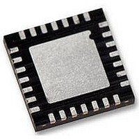
PIC16F1827-I/MQ Microchip Technology, PIC16F1827-I/MQ Datasheet - Page 117

PIC16F1827-I/MQ
Manufacturer Part Number
PIC16F1827-I/MQ
Description
IC, 8BIT MCU, PIC16F, 32MHZ, QFN-28
Manufacturer
Microchip Technology
Datasheet
1.PIC16LF1827-ISS.pdf
(400 pages)
Specifications of PIC16F1827-I/MQ
Controller Family/series
PIC16F
Eeprom Memory Size
256Byte
Ram Memory Size
384Byte
Cpu Speed
32MHz
No. Of Timers
5
Interface
EUSART, I2C, SPI
Core Size
8 Bit
Program Memory Size
4 Kwords
Processor Series
PIC16F
Core
PIC
Data Bus Width
8 bit
Program Memory Type
Flash
Data Ram Size
384 B
Interface Type
I2C, SPI, UART
Maximum Clock Frequency
32 MHz
Number Of Programmable I/os
15
Number Of Timers
5
Maximum Operating Temperature
+ 85 C
Mounting Style
SMD/SMT
Package / Case
QFN EP
3rd Party Development Tools
52715-96, 52716-328, 52717-734
Development Tools By Supplier
PG164130, DV164035, DV244005, DV164005
Minimum Operating Temperature
- 40 C
On-chip Adc
10 bit, 12 Channel
Lead Free Status / Rohs Status
Details
- Current page: 117 of 400
- Download datasheet (7Mb)
12.0
Depending on the device selected and peripherals
enabled, there are two ports available. In general,
when a peripheral is enabled, that pin may not be used
as a general purpose I/O pin.
Each port has three registers for its operation. These
registers are:
• TRISx registers (data direction register)
• PORTx registers (reads the levels on the pins of
• LATx registers (output latch)
The Data Latch (LATx registers) is useful for
read-modify-write operations on the value that the I/O
pins are driving.
A write operation to the LATx register has the same
affect as a write to the corresponding PORTx register.
A read of the LATx register reads of the values held in
the I/O PORT latches, while a read of the PORTx
register reads the actual I/O pin value.
Ports with analog functions also have an ANSELx
register which can disable the digital input and save
power. A simplified model of a generic I/O port, without
the interfaces to other peripherals, is shown in
Figure 12-1.
FIGURE 12-1:
© 2009 Microchip Technology Inc.
To peripherals
Write LATx
Write PORTx
Data Bus
the device)
Read PORTx
I/O PORTS
Data Register
D
CK
Read LATx
ANSELx
GENERIC I/O PORT
OPERATION
Q
TRISx
V
V
DD
SS
I/O pin
Preliminary
12.1
The Alternate Pin Function Control (APFCONx)
registers are used to steer specific peripheral input and
output functions between different pins. The APFCONx
registers
Register 12-2. For this device family, the following
functions can be moved between different pins.
• RX/DT
• SDO1
• SS1 (Slave Select 1)
• P2B
• CCP2/P2A
• P1D
• P1C
• CCP1/P1A
• TX/CK
These bits have no effect on the values of any TRIS
register. PORT and TRIS overrides will be routed to the
correct pin. The unselected pin will be unaffected.
PIC16F/LF1826/27
Alternate Pin Function
are
shown
in
Register 12-1
DS41391B-page 117
and
Related parts for PIC16F1827-I/MQ
Image
Part Number
Description
Manufacturer
Datasheet
Request
R

Part Number:
Description:
IC, 8BIT MCU, PIC16F, 32MHZ, SOIC-18
Manufacturer:
Microchip Technology
Datasheet:

Part Number:
Description:
IC, 8BIT MCU, PIC16F, 32MHZ, SSOP-20
Manufacturer:
Microchip Technology
Datasheet:

Part Number:
Description:
IC, 8BIT MCU, PIC16F, 32MHZ, DIP-18
Manufacturer:
Microchip Technology
Datasheet:

Part Number:
Description:
IC, 8BIT MCU, PIC16F, 32MHZ, QFN-28
Manufacturer:
Microchip Technology
Datasheet:

Part Number:
Description:
IC, 8BIT MCU, PIC16F, 32MHZ, QFN-28
Manufacturer:
Microchip Technology
Datasheet:

Part Number:
Description:
IC, 8BIT MCU, PIC16F, 32MHZ, QFN-28
Manufacturer:
Microchip Technology
Datasheet:

Part Number:
Description:
IC, 8BIT MCU, PIC16F, 32MHZ, SSOP-20
Manufacturer:
Microchip Technology
Datasheet:

Part Number:
Description:
IC, 8BIT MCU, PIC16F, 20MHZ, DIP-40
Manufacturer:
Microchip Technology
Datasheet:

Part Number:
Description:
IC, 8BIT MCU, PIC16F, 20MHZ, MQFP-44
Manufacturer:
Microchip Technology
Datasheet:

Part Number:
Description:
IC, 8BIT MCU, PIC16F, 20MHZ, QFN-20
Manufacturer:
Microchip Technology
Datasheet:

Part Number:
Description:
IC, 8BIT MCU, PIC16F, 32MHZ, QFN-28
Manufacturer:
Microchip Technology
Datasheet:

Part Number:
Description:
MCU 14KB FLASH 768B RAM 64-TQFP
Manufacturer:
Microchip Technology
Datasheet:

Part Number:
Description:
7 KB Flash, 384 Bytes RAM, 32 MHz Int. Osc, 16 I/0, Enhanced Mid Range Core, Low
Manufacturer:
Microchip Technology

Part Number:
Description:
14KB Flash, 512B RAM, 256B EEPROM, LCD, 1.8-5.5V 40 UQFN 5x5x0.5mm TUBE
Manufacturer:
Microchip Technology
Datasheet:

Part Number:
Description:
14KB Flash, 512B RAM, 256B EEPROM, LCD, 1.8-5.5V 40 UQFN 5x5x0.5mm TUBE
Manufacturer:
Microchip Technology


