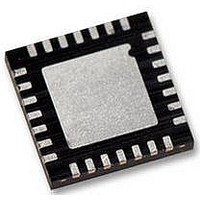
PIC16F1827-I/MQ Microchip Technology, PIC16F1827-I/MQ Datasheet - Page 226

PIC16F1827-I/MQ
Manufacturer Part Number
PIC16F1827-I/MQ
Description
IC, 8BIT MCU, PIC16F, 32MHZ, QFN-28
Manufacturer
Microchip Technology
Datasheet
1.PIC16LF1827-ISS.pdf
(400 pages)
Specifications of PIC16F1827-I/MQ
Controller Family/series
PIC16F
Eeprom Memory Size
256Byte
Ram Memory Size
384Byte
Cpu Speed
32MHz
No. Of Timers
5
Interface
EUSART, I2C, SPI
Core Size
8 Bit
Program Memory Size
4 Kwords
Processor Series
PIC16F
Core
PIC
Data Bus Width
8 bit
Program Memory Type
Flash
Data Ram Size
384 B
Interface Type
I2C, SPI, UART
Maximum Clock Frequency
32 MHz
Number Of Programmable I/os
15
Number Of Timers
5
Maximum Operating Temperature
+ 85 C
Mounting Style
SMD/SMT
Package / Case
QFN EP
3rd Party Development Tools
52715-96, 52716-328, 52717-734
Development Tools By Supplier
PG164130, DV164035, DV244005, DV164005
Minimum Operating Temperature
- 40 C
On-chip Adc
10 bit, 12 Channel
Lead Free Status / Rohs Status
Details
- Current page: 226 of 400
- Download datasheet (7Mb)
PIC16F/LF1826/27
23.6.6
In half-bridge applications where all power switches are
modulated at the PWM frequency, the power switches
normally require more time to turn off than to turn on. If
both the upper and lower power switches are switched
at the same time (one turned on, and the other turned
off), both switches may be on for a short period of time
until one switch completely turns off. During this brief
interval, a very high current (shoot-through current) will
flow through both power switches, shorting the bridge
supply.
shoot-through current from flowing during switching,
turning on either of the power switches is normally
delayed to allow the other switch to completely turn off.
In Half-Bridge mode, a digitally programmable
dead-band delay is available to avoid shoot-through
current from destroying the bridge power switches. The
delay occurs at the signal transition from the non-active
state to the active state. See Figure 23-16 for
illustration. The lower seven bits of the associated
PWMxCON register (Register 23-4) sets the delay
period in terms of microcontroller instruction cycles
(T
FIGURE 23-17:
DS41391B-page 226
CY
Standard Half-Bridge Circuit (“Push-Pull”)
or 4 T
To
OSC
PROGRAMMABLE DEAD-BAND
DELAY MODE
).
avoid
EXAMPLE OF HALF-BRIDGE APPLICATIONS
this
potentially
P1A
P1B
destructive
Preliminary
FET
Driver
FET
Driver
FIGURE 23-16:
P1A
P1B
td = Dead-Band Delay
Note 1: At this time, the TMRx register is equal to the
(2)
(2)
V+
V-
(1)
2: Output signals are shown as active-high.
td
Pulse Width
PRx register.
Load
Period
td
EXAMPLE OF
HALF-BRIDGE PWM
OUTPUT
© 2009 Microchip Technology Inc.
+
V
-
+
V
-
(1)
Period
(1)
Related parts for PIC16F1827-I/MQ
Image
Part Number
Description
Manufacturer
Datasheet
Request
R

Part Number:
Description:
IC, 8BIT MCU, PIC16F, 32MHZ, SOIC-18
Manufacturer:
Microchip Technology
Datasheet:

Part Number:
Description:
IC, 8BIT MCU, PIC16F, 32MHZ, SSOP-20
Manufacturer:
Microchip Technology
Datasheet:

Part Number:
Description:
IC, 8BIT MCU, PIC16F, 32MHZ, DIP-18
Manufacturer:
Microchip Technology
Datasheet:

Part Number:
Description:
IC, 8BIT MCU, PIC16F, 32MHZ, QFN-28
Manufacturer:
Microchip Technology
Datasheet:

Part Number:
Description:
IC, 8BIT MCU, PIC16F, 32MHZ, QFN-28
Manufacturer:
Microchip Technology
Datasheet:

Part Number:
Description:
IC, 8BIT MCU, PIC16F, 32MHZ, QFN-28
Manufacturer:
Microchip Technology
Datasheet:

Part Number:
Description:
IC, 8BIT MCU, PIC16F, 32MHZ, SSOP-20
Manufacturer:
Microchip Technology
Datasheet:

Part Number:
Description:
IC, 8BIT MCU, PIC16F, 20MHZ, DIP-40
Manufacturer:
Microchip Technology
Datasheet:

Part Number:
Description:
IC, 8BIT MCU, PIC16F, 20MHZ, MQFP-44
Manufacturer:
Microchip Technology
Datasheet:

Part Number:
Description:
IC, 8BIT MCU, PIC16F, 20MHZ, QFN-20
Manufacturer:
Microchip Technology
Datasheet:

Part Number:
Description:
IC, 8BIT MCU, PIC16F, 32MHZ, QFN-28
Manufacturer:
Microchip Technology
Datasheet:

Part Number:
Description:
MCU 14KB FLASH 768B RAM 64-TQFP
Manufacturer:
Microchip Technology
Datasheet:

Part Number:
Description:
7 KB Flash, 384 Bytes RAM, 32 MHz Int. Osc, 16 I/0, Enhanced Mid Range Core, Low
Manufacturer:
Microchip Technology

Part Number:
Description:
14KB Flash, 512B RAM, 256B EEPROM, LCD, 1.8-5.5V 40 UQFN 5x5x0.5mm TUBE
Manufacturer:
Microchip Technology
Datasheet:

Part Number:
Description:
14KB Flash, 512B RAM, 256B EEPROM, LCD, 1.8-5.5V 40 UQFN 5x5x0.5mm TUBE
Manufacturer:
Microchip Technology


