PIC16F1827-I/MQ Microchip Technology, PIC16F1827-I/MQ Datasheet - Page 22
PIC16F1827-I/MQ
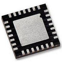
Manufacturer Part Number
PIC16F1827-I/MQ
Description
IC, 8BIT MCU, PIC16F, 32MHZ, QFN-28
Manufacturer
Microchip Technology
Datasheet
1.PIC16LF1827-ISS.pdf
(400 pages)
Specifications of PIC16F1827-I/MQ
Controller Family/series
PIC16F
Eeprom Memory Size
256Byte
Ram Memory Size
384Byte
Cpu Speed
32MHz
No. Of Timers
5
Interface
EUSART, I2C, SPI
Core Size
8 Bit
Program Memory Size
4 Kwords
Processor Series
PIC16F
Core
PIC
Data Bus Width
8 bit
Program Memory Type
Flash
Data Ram Size
384 B
Interface Type
I2C, SPI, UART
Maximum Clock Frequency
32 MHz
Number Of Programmable I/os
15
Number Of Timers
5
Maximum Operating Temperature
+ 85 C
Mounting Style
SMD/SMT
Package / Case
QFN EP
3rd Party Development Tools
52715-96, 52716-328, 52717-734
Development Tools By Supplier
PG164130, DV164035, DV244005, DV164005
Minimum Operating Temperature
- 40 C
On-chip Adc
10 bit, 12 Channel
Lead Free Status / Rohs Status
Details


PIC16F/LF1826/27
3.1.1.2
The program memory can be accessed as data by set-
ting bit 7 of the FSRxH register and reading the match-
ing INDFx register. The MOVIW instruction will place the
lower 8 bits of the addressed word in the W register.
Writes to the program memory cannot be performed via
the INDF registers. Instructions that access the pro-
gram memory via the FSR require one extra instruction
cycle to complete. Example 3-2 demonstrates access-
ing the program memory via an FSR.
The HIGH directive will set bit<7> if a label points to a
location in program memory.
EXAMPLE 3-2:
3.2
The data memory is partitioned in 32 memory banks
with 128 bytes in a bank. Each bank consists of
(Figure 3-3):
• 12 core registers
• 20 Special Function Registers (SFR)
• Up to 80 bytes of General Purpose RAM (GPR)
• 16 bytes of common RAM
The active bank is selected by writing the bank number
into the Bank Select Register (BSR). Unimplemented
memory will read as ‘0’. All data memory can be
accessed either directly (via instructions that use the
file registers) or indirectly via the two File Select
Registers
Addressing” for more information.
DS41391B-page 22
constants
my_function
;THE PROGRAM MEMORY IS IN W
RETLW DATA0
RETLW DATA1
RETLW DATA2
RETLW DATA3
;… LOTS OF CODE…
MOVLW
MOVWF
MOVLW
MOVWF
MOVIW 0[INDF1]
Data Memory Organization
(FSR).
Indirect Read with FSR
LOW constants
FSR1L
HIGH constants
FSR1H
ACCESSING PROGRAM
MEMORY VIA FSR
See
;Index0 data
;Index1 data
Section 3.5
“Indirect
Preliminary
3.2.1
The core registers contain the registers that directly
affect the basic operation of the PIC16F/LF1826/27.
These registers are listed below:
• INDF0
• INDF1
• PCL
• STATUS
• FSR0 Low
• FSR0 High
• FSR1 Low
• FSR1 High
• BSR
• WREG
• PCLATH
• INTCON
Note:
CORE REGISTERS
The core registers are the first 12
addresses of every data memory bank.
© 2009 Microchip Technology Inc.
Related parts for PIC16F1827-I/MQ
Image
Part Number
Description
Manufacturer
Datasheet
Request
R

Part Number:
Description:
IC, 8BIT MCU, PIC16F, 32MHZ, SOIC-18
Manufacturer:
Microchip Technology
Datasheet:

Part Number:
Description:
IC, 8BIT MCU, PIC16F, 32MHZ, SSOP-20
Manufacturer:
Microchip Technology
Datasheet:

Part Number:
Description:
IC, 8BIT MCU, PIC16F, 32MHZ, DIP-18
Manufacturer:
Microchip Technology
Datasheet:

Part Number:
Description:
IC, 8BIT MCU, PIC16F, 32MHZ, QFN-28
Manufacturer:
Microchip Technology
Datasheet:

Part Number:
Description:
IC, 8BIT MCU, PIC16F, 32MHZ, QFN-28
Manufacturer:
Microchip Technology
Datasheet:
Part Number:
Description:
IC, 8BIT MCU, PIC16F, 32MHZ, QFN-28
Manufacturer:
Microchip Technology
Datasheet:
Part Number:
Description:
IC, 8BIT MCU, PIC16F, 32MHZ, SSOP-20
Manufacturer:
Microchip Technology
Datasheet:

Part Number:
Description:
IC, 8BIT MCU, PIC16F, 20MHZ, DIP-40
Manufacturer:
Microchip Technology
Datasheet:

Part Number:
Description:
IC, 8BIT MCU, PIC16F, 20MHZ, MQFP-44
Manufacturer:
Microchip Technology
Datasheet:

Part Number:
Description:
IC, 8BIT MCU, PIC16F, 20MHZ, QFN-20
Manufacturer:
Microchip Technology
Datasheet:
Part Number:
Description:
IC, 8BIT MCU, PIC16F, 32MHZ, QFN-28
Manufacturer:
Microchip Technology
Datasheet:

Part Number:
Description:
MCU 14KB FLASH 768B RAM 64-TQFP
Manufacturer:
Microchip Technology
Datasheet:
Part Number:
Description:
7 KB Flash, 384 Bytes RAM, 32 MHz Int. Osc, 16 I/0, Enhanced Mid Range Core, Low
Manufacturer:
Microchip Technology

Part Number:
Description:
14KB Flash, 512B RAM, 256B EEPROM, LCD, 1.8-5.5V 40 UQFN 5x5x0.5mm TUBE
Manufacturer:
Microchip Technology
Datasheet:
Part Number:
Description:
14KB Flash, 512B RAM, 256B EEPROM, LCD, 1.8-5.5V 40 UQFN 5x5x0.5mm TUBE
Manufacturer:
Microchip Technology