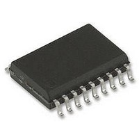
ST62T15CM6 STMicroelectronics, ST62T15CM6 Datasheet - Page 42

ST62T15CM6
Manufacturer Part Number
ST62T15CM6
Description
8BIT MCU OTP 2K, SMD, 62T15, SOIC20
Manufacturer
STMicroelectronics
Datasheet
1.ST62T15CB6.pdf
(105 pages)
Specifications of ST62T15CM6
Controller Family/series
ST6
Core Size
8bit
No. Of I/o's
20
Program Memory Size
2KB
Ram Memory Size
64Byte
Cpu Speed
8MHz
Oscillator Type
External Only
No. Of Timers
1
Digital Ic Case
RoHS Compliant
Peripherals
ADC,
Rohs Compliant
No
Processor Series
ST62T1x
Core
ST6
Data Bus Width
8 bit
Program Memory Type
EPROM
Data Ram Size
64 B
Maximum Clock Frequency
8 MHz
Number Of Programmable I/os
20
Number Of Timers
2
Operating Supply Voltage
3 V to 6 V
Maximum Operating Temperature
+ 85 C
Mounting Style
SMD/SMT
Package / Case
SOP-28
Development Tools By Supplier
ST62GP-EMU2, ST62E2XC-EPB/110, ST62E6XC-EPB/US, STREALIZER-II
Minimum Operating Temperature
- 40 C
On-chip Adc
8 bit
Lead Free Status / Rohs Status
In Transition
Available stocks
Company
Part Number
Manufacturer
Quantity
Price
Company:
Part Number:
ST62T15CM6
Manufacturer:
STM
Quantity:
2 508
Part Number:
ST62T15CM6
Manufacturer:
ST
Quantity:
20 000
ST6215C/ST6225C
I/O PORTS (Cont’d)
8.5 REGISTER DESCRIPTION
DATA REGISTER (DR)
Port x Data Register
DRx with x = A, B or C.
Addresses 0C0h, 0C1h and 0C2h- Read /Write
Reset Value: 0000 0000 (00h)
Bits 7:0 = DR[7:0] Data register bits.
Reading the DR register returns either the DR reg-
ister latch content (pin configured as output) or the
digital value applied to the I/O pin (pin configured
as input).
Caution: In input mode, modifying this register will
modify the I/O port configuration (see
Do not use the Single bit instructions on I/O port
data registers. See
DATA DIRECTION REGISTER (DDR)
Port x Data Direction Register
DDRx with x = A, B or C.
Addresses: 0C4h, 0C5h and 0C6h - Read /Write
Reset Value: 0000 0000 (00h)
Table 10. I/O Port Register Map and Reset Values
42/105
1
DDR7 DDR6 DDR5 DDR4 DDR3 DDR2 DDR1 DDR0
DR7
Address
of all I/O port registers
7
7
(Hex.)
0CCh
0CDh
0C5h
0C6h
0CEh
0C0h
0C1h
0C2h
0C4h
Reset Value
DR6
DRA
DRB
DRC
DDRA
DDRB
DDRC
ORA
ORB
ORC
DR5
Register
Label
(Section
DR4
DR3
MSB
MSB
MSB
8.2.5).
7
0
DR2
Table
DR1
6
0
8).
DR0
0
0
5
0
Bits 7:0 = DDR[7:0] Data direction register bits.
The DDR register gives the input/output direction
configuration of the pins. Each bit is set and
cleared by software.
0: Input mode
1: Output mode
OPTION REGISTER (OR)
Port x Option Register
ORx with x = A, B or C.
Addresses: 0CCh, 0CDh and 0CEh - Read /Write
Reset Value: 0000 0000 (00h)
Bits 7:0 = OR[7:0] Option register bits.
The OR register allows to distinguish in output
mode if the push-pull or open drain configuration is
selected.
Output mode:
0: Open drain output(with P-Buffer deactivated)
1: Push-pull Output
Input mode: See
Each bit is set and cleared by software.
Caution: Modifying this register, will also modify
the I/O port configuration in input mode. (see
ble
OR7
7
8).
4
0
OR6
OR5
3
0
Table
OR4
8.
2
0
OR3
OR2
1
0
OR1
LSB
LSB
LSB
OR0
0
0
0
Ta-


