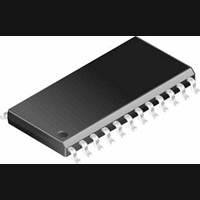
CS5524-AS Cirrus Logic Inc, CS5524-AS Datasheet - Page 14

CS5524-AS
Manufacturer Part Number
CS5524-AS
Description
A/D Converter (A-D) IC
Manufacturer
Cirrus Logic Inc
Datasheet
1.CS5524-AS.pdf
(56 pages)
Specifications of CS5524-AS
Sample Rate
606SPS
Input Channels Per Adc
4
Mounting Type
Surface Mount
No. Of Channels
4
Power Rating
9mW
Peak Reflow Compatible (260 C)
No
Supply Voltage Max
5.25V
Lead Free Status / RoHS Status
Contains lead / RoHS non-compliant
Available stocks
Company
Part Number
Manufacturer
Quantity
Price
Part Number:
CS5524-ASZ
Manufacturer:
CIRRUS
Quantity:
20 000
2.1.1 Instrumentation Amplifier
The instrumentation amplifier is chopper stabilized
and is activated any time conversions are performed
with the low level input ranges, 100 mV. The am-
plifier is powered from VA+ and from the NBV
(Negative
CS5521/22/23/24/28 to be operated in either of two
analog input configurations. The NBV pin can be bi-
ased to a negative voltage between -1.8 V and -
2.5 V, or tied to AGND (for the CS5528, NBV has
to be between -1.8 V and -2.5 V for the ranges below
100 mV when the amplifier is engaged). The com-
mon-mode plus signal range of the instrumentation
amplifier is 1.85 V to 2.65 V with NBV grounded.
The common-mode plus signal range of the instru-
mentation amplifier is -0.150 V to 0.950 V with
NBV between -1.8 V to -2.5 V. Whether NBV is
tied between -1.8 V and -2.5 V or tied to AGND,
the (Common Mode + Signal) input on AIN+ and
AIN- must stay between NBV and VA+.
Figure 5 illustrates an analog input model for the
ADCs when the instrumentation amplifier is en-
gaged. The CVF (sampling) input current for each
of the analog input pins depends on the CFS1 and
CFS0 (Chop Frequency Select) bits in the configu-
ration register (see Configuration Register for de-
tails). Note that the CVF current is lowest with the
14
Figure 5. Input Models for AIN+ and AIN- pins,
V
i = fV
n
os
AIN
25 mV
os
25 mV, 55 mV, and 100 mV Ranges
CFS1/CFS0 = 00, f = 256 Hz
CFS1/CFS0 = 01, f = 4096 Hz
CFS1/CFS0 = 10, f = 16.384 kHz
CFS1/CFS0 = 11, f = 1024 Hz
C
Bias
(100 mV Input Ranges
Voltage)
C = 48 pF
pin
allowing
the
CFS bits in their default states (cleared to logic 0s).
Further note that the CVF current into the instru-
mentation amplifier is less than 300 pA over -40°C
to +85°C. Note that Figure 5 is for input current
modeling only. For physical input capacitance see
‘Input Capacitance’ specification under ANALOG
CHARACTERISTICS. Also refer to Applications
Note AN30 “Switched-Capacitor A/D Converter
Input Structures” for more details on input models
and input sampling currents.
Note: Residual noise appears in the converter’s baseband for
2.1.2 Coarse/Fine Charge Buffers
The unity gain buffers are activated any time conver-
sions are performed with the high level inputs rang-
es, 1 V, 2.5 V, and 5 V. The unity gain buffers are
designed to accommodate rail to rail input signals.
The common-mode plus signal range for the unity
gain buffer amplifier is NBV to VA+.
Typical CVF (sampling) current for the unity gain
buffer
(XIN = 32.768 kHz, see Figure 6).
Figure 6. Input Models for AIN+ and AIN- pins,
V
i = fV
n
output word rates greater than 61.6 Hz if the CFS bits
are logic 0 (chop clock = 256 Hz). For word rates of
30 Hz and lower, 256 Hz chopping is recommended,
and for 61.6 Hz, 84.5 Hz and 101.1 Hz filters, 4096 Hz
chopping is recommended.
os
AIN
25 mV
os
amplifiers
C
1 V, 2.5 V and 5 V Ranges
>100 mV input ranges
f = 32.768 kHz
CS5521/22/23/24/28
is
1
C = 20 pF
Coarse
1
Fine
about
DS317F2
10 nA


