ADIS16130AMLZ Analog Devices Inc, ADIS16130AMLZ Datasheet - Page 9
ADIS16130AMLZ
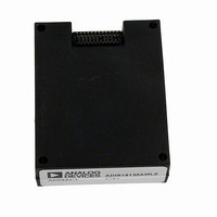
Manufacturer Part Number
ADIS16130AMLZ
Description
MODULE GYRO RATE SENSOR 24LD
Manufacturer
Analog Devices Inc
Datasheet
1.ADIS16130AMLZ.pdf
(16 pages)
Specifications of ADIS16130AMLZ
Range °/s
±250°/s
Sensitivity
23,488LSB/°/s
Typical Bandwidth
300Hz
Voltage - Supply
4.75 V ~ 5.25 V
Current - Supply
73mA
Output Type
Digital
Operating Temperature
-40°C ~ 85°C
Package / Case
Module
No. Of Axes
1
Sensor Case Style
ML-24-3
No. Of Pins
24
Supply Voltage Range
4.75V To 5.25V
Operating Temperature Range
-40°C To +85°C
Msl
MSL 1 - Unlimited
Acceleration Range
2000g
Lead Free Status / RoHS Status
Lead free / RoHS Compliant
Lead Free Status / RoHS Status
Lead free / RoHS Compliant, Lead free / RoHS Compliant
Available stocks
Company
Part Number
Manufacturer
Quantity
Price
Company:

Part Number:
ADIS16130AMLZ
Manufacturer:
SENSIRIO
Quantity:
10 000


BASIC OPERATION
The ADIS16130 produces digital angular rate (RATE) and
temperature (TEMP) data. The digital communication employs
a simple 4-wire SPI that provides access to output data and
several configuration features. A set of communication and
configuration registers govern the operation in the ADIS16130.
See Table 10 for a summary of these registers.
QUICK START
The ADIS16130 SPI operates in 8-bit segments. The first byte of
a SPI sequence goes into the COM register, which contains the
read/write control bit and the address of the target register. When
writing information into control registers, the next byte contains
the configuration information. When reading output data, the
next one to three bytes contain the contents of the register selected.
Configuration Sequence
The sequence in Table 6 provides the recommended configuration
sequence. Table 2 and Figure 2 provide the timing information
for each segment of this configuration sequence.
For additional information on design and optimization with the
ADIS16130, see the AN-1042 Application Note.
Table 6. Configuration Sequence
Step
1
2
3
4
5
6
7
8
9
10
11
12
1
The SDI column lists the hexadecimal code representation of the SDI bit
input sequence.
SDI
0x01
0x38
0x28
0x0A
0x30
0x05
0x2A
0x0A
0x32
0x05
0x38
0x22
1
Register
COM
IOP
COM
RATECS
COM
RATECONV
COM
TEMPCS
COM
TEMPCONV
COM
MODE
Purpose
Start a write sequence for IOP.
Configure the data-ready signal to
pulse low when the RATEDATA and
TEMPDATA output registers
contain new data. The data-ready
signal goes high after reading
either of these registers.
Start a write sequence for the
RATECS register.
Enable and configure the
gyroscope data channel.
Start a write sequence for
RATECONV register.
Initialize the RATE conversion.
Start a write sequence for the
TEMPCS register.
Enable and configure the
temperature data channel.
Start a write sequence for
TEMPCONV.
Initialize the TEMP conversion.
Start a write sequence for the
MODE register.
Establish the data output
resolution to 24 bits and start the
conversion process with the
RATEDATA channel.
Rev. B | Page 9 of 16
Reading RATE Output Data
After the configuration sequence in Table 6 is complete, reading the
output data is very simple. The ADIS16130 converts the RATE
and TEMP data continuously. To better understand this process,
Figure 13 provides an example read sequence, and Table 2 and
Figure 3 provide critical timing details for the output signal. The
first byte of the sequence uses SDI to establish a read of the
RATE output register. This is accomplished by writing 0x48 to the
COM register. The most significant byte is first in the SDO
sequence, followed by the next significant, and then the least
significant. When 16-bit resolution is in use, only two bytes are
output from the SDO during the read sequence.
SCLK
The data-ready signal, RDY , indicates that unread data is
available on both RATE and TEMP output registers. After the
RATE or TEMP channel is read, the signal returns high, as
shown in
sequentially, and each has a sample rate of 5.7 kSPS. The
internal sample rate is not dependent on the SPI signals or read
rates. Using the data-ready signal to drive data collection helps
avoid losing data due to data collision, which is when a user-
driven read cycle coincides with the internal update time. In
this case, the old data remains and the new data is lost.
If a lower sample rate meets system-level requirements, the
data-ready signal can still be useful in facilitating SPI read
sequences. In this case, the data-ready signal pulses high for
approximately 26 μs before returning low and then repeats this
pattern at two times the internal sample rate. This signal can
feed a counter circuit (or firmware), which drives a processor
interrupt routine at a reduced sample rate.
Reading TEMP Output Data
Reading TEMP data requires a sequence that is very similar to
that of Figure 13, except that the initial SDI sequence must be
changed from 0x48 to 0x4A. If the TEMP data is not used, Step 7
to Step 10 of the configuration sequence are not required.
SDO
RDY
SDI
CS
Figure 13
0x48
Figure 13. Read Sequence Example
. The RATE and TEMP channels update
DATA
DATA
ADIS16130
DATA
Related parts for ADIS16130AMLZ
Image
Part Number
Description
Manufacturer
Datasheet
Request
R

Part Number:
Description:
±1.7g Dual-Axis IMEMS Accelerometer Evaluation Board
Manufacturer:
Analog Devices Inc
Datasheet:

Part Number:
Description:
Inertial Sensor Evaluation System
Manufacturer:
Analog Devices Inc
Datasheet:
Part Number:
Description:
Manufacturer:
Analog Devices Inc
Datasheet:
Part Number:
Description:
Manufacturer:
Analog Devices Inc
Datasheet:
Part Number:
Description:
Manufacturer:
Analog Devices Inc
Datasheet:
Part Number:
Description:
Manufacturer:
Analog Devices Inc
Datasheet:
Part Number:
Description:
Manufacturer:
Analog Devices Inc
Datasheet:
Part Number:
Description:
Manufacturer:
Analog Devices Inc
Datasheet:
Part Number:
Description:
Manufacturer:
Analog Devices Inc
Datasheet:
Part Number:
Description:
Manufacturer:
Analog Devices Inc
Datasheet:
Part Number:
Description:
Manufacturer:
Analog Devices Inc
Datasheet:
Part Number:
Description:
Manufacturer:
Analog Devices Inc
Datasheet:
Part Number:
Description:
Manufacturer:
Analog Devices Inc
Datasheet: