2SK3934 Toshiba, 2SK3934 Datasheet
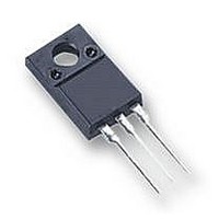
MOSFET, N, 500V, TO-220SIS

2SK3934

Manufacturer Part Number
2SK3934
Description
MOSFET, N, 500V, TO-220SIS
Manufacturer
Toshiba
Datasheet

Specifications of 2SK3934

Transistor Polarity
N Channel
Continuous Drain Current Id
15A
Drain Source Voltage Vds
500V
On Resistance Rds(on)
300mohm
Rds(on) Test Voltage Vgs
10V
Voltage Vgs Max
30V
Transistor Case
RoHS Compliant
Threshold Voltage Vgs Typ
4V
Rohs Compliant
Yes

Available stocks

Company
Part Number
Manufacturer
Quantity
Price
Part Number:
2SK3934
Manufacturer:
TOSHIBAHIBA
Quantity:
12 500
Part Number:
2SK3934
Manufacturer:
TOSHIBA
Quantity:
216
Part Number:
2SK3934
Manufacturer:
TOSHIBA/东芝
Quantity:
20 000
Company:
Part Number:
2SK3934
Quantity:
50
Switching Regulator Applications
Maximum Ratings
Thermal Characteristics
This transistor is an electrostatic-sensitive device. Handle with care.
Low drain-source ON resistance: R
High forward transfer admittance: |Y
Low leakage current: I
Enhancement model: V
Drain-source voltage
Drain-gate voltage (R
Gate-source voltage
Drain current
Drain power dissipation (Tc = 25°C)
Single pulse avalanche energy
Avalanche current
Repetitive avalanche energy (Note 3)
Channel temperature
Storage temperature range
Thermal resistance, channel to case
Thermal resistance, channel to ambient
Note 1: Ensure that the channel temperature does not exceed 150°C during use of the device.
Note 2: V
Note 3: Repetitive rating: pulse width limited by maximum channel temperature
DD
Characteristic
TOSHIBA Field Effect Transistor Silicon N-Channel MOS Type (π-MOSVI)
Characteristic
= 90 V, T
GS
DC
Pulse (t = 1 ms)
= 20 kΩ)
(Ta = 25°C)
ch
DSS
th
= 25°C (initial), L = 8.16mH, I
(Note 1)
(Note 1)
(Note 2)
= 2.0~4.0 V (V
= 100 µA (V
DS (ON)
Symbol
V
V
V
fs
E
E
T
I
I
T
P
DS
DGR
GSS
DSS
I
DP
AR
AR
stg
| = 8.2 S (typ.)
AS
D
ch
R
DS
D
R
2SK3934
Symbol
th (ch-c)
th (ch-a)
= 500 V)
= 0.23Ω (typ.)
= 10 V, I
-55~150
Rating
D
1.08
500
500
±30
150
5.0
AR
15
60
50
15
1
= 1 mA)
Max
62.5
2.5
= 15 A, R
Unit
G
mJ
°C/W
°C/W
°C
°C
W
V
V
V
A
A
Unit
J
= 25 Ω
Weight: 1.7 g (typ.)
JEDEC
JEITA
TOSHIBA
1
1: Gate
2: Drain
3: Source
2-10U1B
SC-67
2005-01-24
2SK3934
2
3
Unit: mm

Related parts for 2SK3934

2SK3934 Summary of contents

Page 1

... DS D Symbol Rating Unit V 500 V DSS V 500 V DGR ± GSS 1. 5 150 ° -55~150 °C stg Symbol Max Unit R 2.5 °C/W th (ch-c) R 62.5 °C/W th (ch- Ω 2SK3934 Unit Gate 2: Drain 3: Source JEDEC ― JEITA SC-67 TOSHIBA 2-10U1B Weight: 1.7 g (typ 2005-01-24 ...

Page 2

... Q gd (Ta = 25°C) Symbol Test Condition ⎯ ⎯ I DRP = DSF /dt = 100 A/ µ 2SK3934 Min Typ. Max Unit ⎯ ⎯ ± 10 µ A ± 30 ⎯ ⎯ V ⎯ ⎯ µ A 100 ⎯ ⎯ 500 V ⎯ 2.0 4.0 V ⎯ Ω 0.23 0.3 ⎯ 2.3 8.2 S ⎯ ...

Page 3

... PULSE TEST DRAIN − SOURCE VOLTAGE GATE − SOURCE VOLTAGE (ON) 1000 100 COMMON SOURCE Tc = 25°C PULSE TEST 10 100 1 DRAIN CURRENT I 3 2SK3934 – 10V 8V 7. (V) DS – COMMON SOURCE Tc = 25℃ PULSE TEST 7 3 (V) GS – 100 (A) D 2005-01-24 ...

Page 4

... COMMON SOURCE rss PULSE TEST 0 −80 −40 100 0 (V) CASE TEMPERATURE Tc (°C) DYNAMIC INPUT/OUTPUT CHARACTERISTICS 500 400 V DS 300 200 V GS 100 0 20 160 0 TOTAL GATE CHARGE Q 4 2SK3934 I – −0.8 −1.2 −1.6 ( – 120 160 100 V 400V 12 200V 8 COMMON SOURCE 25° ...

Page 5

... T Duty = t (ch-c) = 2.5°C/W 10m 100m 1 PULSE WIDTH t ( 1200 1000 800 600 400 200 CHANNEL TEMPERATURE (INITIAL 1000 − TEST CIRCUIT = 25 Ω 8. 2SK3934 10 – 100 125 150 T (° VDSS WAVEFORM ⎛ ⎞ VDSS 2 I ⎜ ⎟ = ⋅ ⋅ ⋅ L Ε AS ⎜ ...

Page 6

... Unintended Usage of TOSHIBA products listed in this document shall be made at the customer’s own risk. • TOSHIBA products should not be embedded to the downstream products which are prohibited to be produced and sold, under any law and regulations. 6 2SK3934 030619EAA 2005-01-24 ...

Related keywords