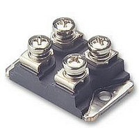
IXFN180N10 IXYS SEMICONDUCTOR, IXFN180N10 Datasheet

IXFN180N10
Manufacturer Part Number
IXFN180N10
Description
N CH MOSFET, 100V, 180A, SOT-227B
Manufacturer
IXYS SEMICONDUCTOR
Datasheet
1.IXFN180N10.pdf
(4 pages)
Specifications of IXFN180N10
Transistor Polarity
N Channel
Continuous Drain Current Id
180A
Drain Source Voltage Vds
100V
On Resistance Rds(on)
8mohm
Rds(on) Test Voltage Vgs
10V
Threshold Voltage Vgs Typ
4V
Lead Free Status / RoHS Status
Lead free / RoHS Compliant
Available stocks
Company
Part Number
Manufacturer
Quantity
Price
Company:
Part Number:
IXFN180N10
Manufacturer:
IXYS
Quantity:
240
Part Number:
IXFN180N10
Quantity:
128
HiPerFET
Power MOSFET
Single MOSFET Die
Preliminary data sheet
© 1999 IXYS All rights reserved
Symbol Test Conditions
V
V
V
V
I
I
I
I
E
E
dv/dt
P
T
T
T
T
V
M
Weight
Symbol
(T
V
V
I
I
R
D25
L(RMS)
DM
AR
GSS
DSS
J
JM
stg
L
DGR
GS
GSM
AR
AS
D
ISOL
DSS
DSS
GS(th)
DS(on)
d
J
= 25 C, unless otherwise specified)
T
T
T
T
Continuous
Transient
Terminal (current limit)
T
T
T
I
T
T
1.6 mm (0.063 in) from case for 10 s
50/60 Hz, RMS
I
Mounting torque
Terminal connection torque
V
V
V
V
V
V
Note 2
S
ISOL
C
C
C
C
J
J
C
J
C
GS
GS
DS
GS
DS
GS
= 25 C
= 25 C
= V
= 25°C to 150°C
= 25°C to 150°C, R
= 25 C;
= 25 C
= 25 C
= 25 C
= 0 V, I
= 20V, V
= 0 V
= V
= 10V, I
Test Conditions
I
150 C, R
DM
1 mA
DSS
GS
, di/dt 100 A/ s, V
, I
D
D
D
= 3mA
= 8mA
= 0.5 • I
GS
TM
Note 1
G
= 0V
= 2
t = 1 min
t = 1 s
D25
GS
= 1M
DD
V
DSS
T
T
J
J
= 25 C
= 125 C
Min.
100
IXFN 180N10
2
Characteristic Values
Typ.
-55 ... +150
-55 ... +150
Maximum Ratings
150
1.5/13 Nm/lb.in.
1.5/13 Nm/lb.in.
2500
3000
100
100
30
180
100
720
180
300
600
20
30
60
Max.
100
100
3
5
2
8
4
V/ns
mJ
m
V~
V~
mA
W
nA
C
C
C
C
A
A
A
V
V
V
V
A
J
g
V
V
A
V
I
R
t
miniBLOC, SOT-227 B (IXFN)
Features
Applications
Advantages
G = Gate
S = Source
D25
rr
International standard package
Encapsulating epoxy meets
UL 94 V-0, flammability classification
miniBLOC with Aluminium nitride
isolation
Low R
Rugged polysilicon gate cell structure
Unclamped Inductive Switching (UIS)
rated
Low package inductance
Fast intrinsic Rectifier
DC-DC converters
Synchronous rectification
Battery chargers
Switched-mode and resonant-mode
power supplies
DC choppers
Temperature and lighting controls
Low voltage relays
Easy to mount
Space savings
High power density
DSS
DS(on)
E153432
250 ns
DS (on)
= 100
= 180
=
HDMOS
D = Drain
8 m
TM
G
process
98546B (8/99)
A
V
S
D
S
Related parts for IXFN180N10
IXFN180N10 Summary of contents
Page 1
TM HiPerFET Power MOSFET Single MOSFET Die Preliminary data sheet Symbol Test Conditions 25°C to 150°C DSS 25°C to 150° DGR Continuous GS V Transient GSM I ...
Page 2
Symbol Test Conditions ( unless otherwise specified 60A, Note iss MHz oss ...
Page 3
Figure 1. Output Characteristics at 25 200 V =10V 150 100 50 0 0.0 0.5 1 Volts DS Figure 3. R normalized to 15A/25 DS(on) 1 10V GS ...
Page 4
Figure 7. Gate Charge 15 V =50V =90A D I =10mA 100 150 200 250 300 350 400 Gate Charge - nC Figure 9. Forward Voltage Drop of the Intrinsic ...


