HW-USB-IIG Xilinx Inc, HW-USB-IIG Datasheet - Page 23
HW-USB-IIG
Manufacturer Part Number
HW-USB-IIG
Description
IC CABLE
Manufacturer
Xilinx Inc
Datasheet
1.HW-USB-II-G.pdf
(35 pages)
Specifications of HW-USB-IIG
Supply Voltage
5.25V
Accessory Type
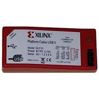
Platform Cable USB II
Ic Cable Type
Download Cable
Connector Type B
USB A Plug
Connector Type A
2-mm Shrouded Keyed Socket
Silicon Family Name
Virtex II, Spartan II
Core Architecture
FPGA
Core Sub-architecture
Virtex, Spartan, XC4000
Rohs Compliant
Yes
Lead Free Status / RoHS Status
Lead free / RoHS Compliant


X-Ref Target - Figure 24
Timing Specifications
For JTAG, SPI, and Slave Serial configuration modes, the TDI_DIN_MOSI and TMS_PROG_SS outputs change on falling
edges of TCK_CCLK_SCK
TCK_CCLK_SCK. The minimum setup time T
where:
Reducing the TCK_CCLK_SCK frequency increases the data setup time at the target.
Note:
the increased propagation delay through the output buffer stage of the cable.
TDO/MISO Timing Considerations
Designers of target systems must take care to observe specific timing requirements for TDO (JTAG chains) or MISO
(dedicated SPI in-system programming) when incorporating the 2-mm IDC connector. In particular, if an open-drain or open-
collector buffer is inserted between TDO (MISO) and the cable, the value of the pull-up resistor at the output of such buffers
must be relatively small (for example, less than 330Ω) to avoid delays associated with parasitic capacitance.
Figure 26, page 25
an internal logic signal not available at the target interface, but is shown to highlight the location of the TDO sampling point.
In
propagates to the cable at G2. The time from G1 to G2 is the sum of the propagation delays in the driver stage of the target
device and the receiver stage of the cable (37 ns in this example).
In
analog representation of the logical condition shown in
DS593 (v1.2.1) March 17, 2011
Figure
Figure
T
T
T
the output stage of the cable.
TSU(MIN)
CLK/2
CPD(MAX)
Timing specifications apply when V
26, the negative TCK transition at G1 causes the last device in the target system JTAG chain to drive TDO, which
27, the cursors show the total setup time (42 ns) before TDO is sampled by the cable.
= TCK_CCLK_SCK low time at 24 MHz,
= Maximum TDI_DIN_MOSI or TMS_PROG_SS propagation delay relative to TCK_CCLK_SCK inherent in
= T
= 20.8 ns – 16.0 ns
= 4.8 ns
and
CLK/2
Figure 27, page 26
– T
(Figure
CPD(MAX)
Figure 24: Enabling the HALT Signal in iMPACT (9.2i)
25). Target devices sample TDI_DIN_MOSI and TMS_PROG_SS on rising edges of
REF
= 3.3V. Operations at 24 MHz might not be possible when using a V
show the timing relationship between TCK and TDO. The signal TDO_SMPL is
TSU(MIN)
www.xilinx.com
for target device sampling of TDI_DIN_MOSI or TMS_PROG_SS is:
Figure 26
and
Figure 27
captured at the target system.
DS593_24_021408
Figure 28, page 27
Platform Cable USB II
REF
below 3.3V due to
is an
23
Related parts for HW-USB-IIG
Image
Part Number
Description
Manufacturer
Datasheet
Request
R

Part Number:
Description:
PLATFORM CABLE USB
Manufacturer:
Xilinx Inc
Datasheet:

Part Number:
Description:
PLATFORM CABLE USB II
Manufacturer:
Xilinx Inc
Datasheet:

Part Number:
Description:
BOARD ADAPTER AND FLY LEADS
Manufacturer:
Xilinx Inc
Datasheet:

Part Number:
Description:
XLXHW-LICENSE-DONGLE-USB-G USB DONGLE OP
Manufacturer:
Xilinx Inc

Part Number:
Description:
IC CPLD .8K 36MCELL 44-VQFP
Manufacturer:
Xilinx Inc
Datasheet:

Part Number:
Description:
IC CPLD 72MCRCELL 10NS 44VQFP
Manufacturer:
Xilinx Inc
Datasheet:

Part Number:
Description:
IC CPLD 1.6K 72MCELL 64-VQFP
Manufacturer:
Xilinx Inc
Datasheet:

Part Number:
Description:
IC CR-II CPLD 64MCELL 44-VQFP
Manufacturer:
Xilinx Inc
Datasheet:

Part Number:
Description:
IC CPLD 1.6K 72MCELL 100-TQFP
Manufacturer:
Xilinx Inc
Datasheet:

Part Number:
Description:
IC CR-II CPLD 64MCELL 56-BGA
Manufacturer:
Xilinx Inc
Datasheet:

Part Number:
Description:
IC CPLD 72MCRCELL 7.5NS 44VQFP
Manufacturer:
Xilinx Inc
Datasheet:
Part Number:
Description:
IC CR-II CPLD 64MCELL 100-VQFP
Manufacturer:
Xilinx Inc
Datasheet:
Part Number:
Description:
IC CPLD 1.6K 72MCELL 100-TQFP
Manufacturer:
Xilinx Inc
Datasheet:

Part Number:
Description:
IC CPLD 72MCRCELL 7.5NS 64VQFP
Manufacturer:
Xilinx Inc
Datasheet:
Part Number:
Description:
IC CPLD 1.6K 72MCELL 100-TQFP
Manufacturer:
Xilinx Inc
Datasheet: