HW-USB-IIG Xilinx Inc, HW-USB-IIG Datasheet - Page 31
HW-USB-IIG
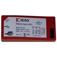
Manufacturer Part Number
HW-USB-IIG
Description
IC CABLE
Manufacturer
Xilinx Inc
Datasheet
1.HW-USB-II-G.pdf
(35 pages)
Specifications of HW-USB-IIG
Supply Voltage
5.25V
Accessory Type
Platform Cable USB II
Ic Cable Type
Download Cable
Connector Type B
USB A Plug
Connector Type A
2-mm Shrouded Keyed Socket
Silicon Family Name
Virtex II, Spartan II
Core Architecture
FPGA
Core Sub-architecture
Virtex, Spartan, XC4000
Rohs Compliant
Yes
Lead Free Status / RoHS Status
Lead free / RoHS Compliant


Table 6: JTAG/SPI/Slave Serial Port: 2-mm Connector Signals (Cont’d)
Platform Cable USB II Operating Characteristics
Table 7: Absolute Maximum Ratings
DS593 (v1.2.1) March 17, 2011
Notes:
1.
2.
3.
4.
3, 5, 7, 9,
Number
Symbol
1, 12
Pin
The listed SPI pin names match those of SPI flash devices from ST Microelectronics. Pin names of compatible SPI devices from other
vendors can vary. Consult the vendor's SPI device data sheet for equivalent pin names.
The signal pins (HALT_INIT_WP, TDI_DIN_MOSI, TDO_DONE_MISO, TCK_CCLK_SCK, TMS_PROG_SS) are bidirectional. Their
directions during cable operations are defined by the current configuration or programming mode (JTAG, SPI or Slave Serial).
The target reference voltage must be regulated and not have a current-limiting resistor in series with the V
For more details, see
V
V
10
13
14
11
I
8
REF
T
BUS
REF
A
Configuration
USB Port Supply Voltage
Target Reference Voltage
Target Supply Current
Ambient Operating Temperature
JTAG
–
–
–
–
–
–
Target System Connections, page 15
Programming
Description
MODE
SPI
–
–
–
–
–
–
(1)
(1)
Configuration
Slave-Serial
PGND
Done
INIT
DIN
www.xilinx.com
–
–
and
Pseudo Ground Signal, page
V
REF
= 5.25V
Direction
Out
Out
In
In
–
–
Conditions
(2)
Slave Serial Configuration Done. This pin
indicates to Platform Cable USB II that
target FPGAs have received the entire
configuration bitstream and should be
connected to the Done pin on all FPGAs in
parallel for daisy-chained configurations.
Additional CCLK cycles are issued following
the positive transition of Done to insure that
the configuration process is complete.
Slave Serial Configuration Data Input.
This pin outputs the serial input data stream
for target FPGAs and should be connected
to the DIN pin of the target FPGA in a single-
device system, or to the DIN pin of the first
FPGA in a daisy-chain configuration.
Slave Serial Pseudo Ground. Use of this
pin is optional. PGND is pulled Low during
Slave Serial operations; otherwise, it is high-
Z. This pin is connected to an open-drain
driver and requires a pull-up resistor on the
target system.
Slave Serial Configuration Initialization.
This pin indicates that configuration memory
is being cleared and should be connected to
the INIT_B pin of the target FPGA for a
single-device system, or to the INIT_B pin
on all FPGAs in parallel in a daisy-chain
configuration.
Digital Ground. All ground pins should be
connected to digital ground on the target
system to minimize crosstalk.
Not Connected.
22.
REF
(4)
Description
pin.
Platform Cable USB II
Value
5.25
6.00
100
70
Units
mA
°
V
V
C
31
Related parts for HW-USB-IIG
Image
Part Number
Description
Manufacturer
Datasheet
Request
R

Part Number:
Description:
PLATFORM CABLE USB
Manufacturer:
Xilinx Inc
Datasheet:

Part Number:
Description:
PLATFORM CABLE USB II
Manufacturer:
Xilinx Inc
Datasheet:

Part Number:
Description:
BOARD ADAPTER AND FLY LEADS
Manufacturer:
Xilinx Inc
Datasheet:

Part Number:
Description:
XLXHW-LICENSE-DONGLE-USB-G USB DONGLE OP
Manufacturer:
Xilinx Inc

Part Number:
Description:
IC CPLD .8K 36MCELL 44-VQFP
Manufacturer:
Xilinx Inc
Datasheet:

Part Number:
Description:
IC CPLD 72MCRCELL 10NS 44VQFP
Manufacturer:
Xilinx Inc
Datasheet:

Part Number:
Description:
IC CPLD 1.6K 72MCELL 64-VQFP
Manufacturer:
Xilinx Inc
Datasheet:

Part Number:
Description:
IC CR-II CPLD 64MCELL 44-VQFP
Manufacturer:
Xilinx Inc
Datasheet:

Part Number:
Description:
IC CPLD 1.6K 72MCELL 100-TQFP
Manufacturer:
Xilinx Inc
Datasheet:

Part Number:
Description:
IC CR-II CPLD 64MCELL 56-BGA
Manufacturer:
Xilinx Inc
Datasheet:

Part Number:
Description:
IC CPLD 72MCRCELL 7.5NS 44VQFP
Manufacturer:
Xilinx Inc
Datasheet:
Part Number:
Description:
IC CR-II CPLD 64MCELL 100-VQFP
Manufacturer:
Xilinx Inc
Datasheet:
Part Number:
Description:
IC CPLD 1.6K 72MCELL 100-TQFP
Manufacturer:
Xilinx Inc
Datasheet:

Part Number:
Description:
IC CPLD 72MCRCELL 7.5NS 64VQFP
Manufacturer:
Xilinx Inc
Datasheet:
Part Number:
Description:
IC CPLD 1.6K 72MCELL 100-TQFP
Manufacturer:
Xilinx Inc
Datasheet: