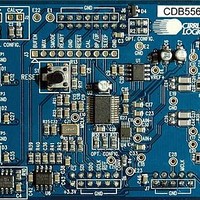
CDB5566 Cirrus Logic Inc, CDB5566 Datasheet - Page 19
CDB5566
Manufacturer Part Number
CDB5566
Description
Dev Bd For I/C 24-bit, Diff, 5kSPS, DAQ
Manufacturer
Cirrus Logic Inc
Type
A/Dr
Specifications of CDB5566
Number Of Adc's
1
Number Of Bits
24
Sampling Rate (per Second)
5k
Data Interface
SPI™
Inputs Per Adc
2 Differential
Input Range
0 ~ 4.096 V
Power (typ) @ Conditions
20mW @ 5kSPS
Voltage Supply Source
Analog and Digital, Dual ±
Operating Temperature
-40°C ~ 85°C
Utilized Ic / Part
CS5566
Conversion Rate
5 KSPS
Resolution
24 bit
Maximum Clock Frequency
8 MHz
Interface Type
SPI
Supply Voltage (max)
3.3 V
Supply Voltage (min)
- 2.5 V
Product
Data Conversion Development Tools
Lead Free Status / RoHS Status
Contains lead / RoHS non-compliant
For Use With/related Products
CS5566
Lead Free Status / RoHS Status
Contains lead / RoHS non-compliant
Other names
598-1557
CDB-5566
CDB-5566


The following figure depicts the CS5566 device powered from a single 5V analog supply.
DS806PP1
47pF
47pF
4.99k
4.99k
49.9
49.9
Reference
(NOTE 1)
Voltage
+4.096
+5 V
Figure 9. CS5566 Configured Using a Single 5V Analog Supply
+0.452 V
+4.548 V
+0.452 V
4.548 V
2.5 V
2.5 V
2.048 V
4.096 V
10 µF
(V+) Buffers On
(V-) Buffers Off
47 µF
4700pF
4700pF
C0G
C0G
0.1 µF
0.1 µF
NOTES
3/25/08
+5 V
1. See Section 3.3 Voltage Reference for information on
2. Locate capacitors so as to minimize loop length.
3. V1-, V2-, and VLR should be connected to the same
4. SCLK and SDO may require pull-down resistors in
BUFEN
VREF+
VREF-
AIN-
AIN+
required voltage reference performance criteria.
ground plane under the chip.
some applications.
0.1 µF
0.1 µF
10
X7R
V1+
V2+
V2-
DCR
V1-
CS5566
SMODE
VLR2
SLEEP
VLR
4
BP/UP
CONV
MCLK
+3.3 V to 1.8 V
SCLK
4
VL
SDO
RDY
RST
TST
CS
0.1 µF
50
CS5566
19
Related parts for CDB5566
Image
Part Number
Description
Manufacturer
Datasheet
Request
R

Part Number:
Description:
Development Kit
Manufacturer:
Cirrus Logic Inc
Datasheet:
Part Number:
Description:
Development Kit
Manufacturer:
Cirrus Logic Inc
Datasheet:


Part Number:
Description:
High-efficiency PFC + Fluorescent Lamp Driver Reference Design
Manufacturer:
Cirrus Logic Inc
Datasheet:
Part Number:
Description:
Development Kit
Manufacturer:
Cirrus Logic Inc
Datasheet:
Part Number:
Description:
Development Kit
Manufacturer:
Cirrus Logic Inc
Datasheet:

Part Number:
Description:
Development Kit
Manufacturer:
Cirrus Logic Inc
Datasheet:
Part Number:
Description:
Development Kit
Manufacturer:
Cirrus Logic Inc
Datasheet:
Part Number:
Description:
Development Kit
Manufacturer:
Cirrus Logic Inc
Datasheet:
Part Number:
Description:
Development Kit
Manufacturer:
Cirrus Logic Inc
Datasheet:

Part Number:
Description:
EVALUATION BOARD FOR CS8427
Manufacturer:
Cirrus Logic Inc
Datasheet:

Part Number:
Description:
BOARD EVAL FOR CS8416 RCVR
Manufacturer:
Cirrus Logic Inc
Datasheet:

Part Number:
Description:
EVALUATION BOARD FOR CS8420
Manufacturer:
Cirrus Logic Inc
Datasheet:

Part Number:
Description:
KIT DEVELOPMENT EP9315 ARM9
Manufacturer:
Cirrus Logic Inc
Datasheet:

Part Number:
Description:
KIT DEVELOPMENT EP9302 ARM9
Manufacturer:
Cirrus Logic Inc
Datasheet: