CDK5560 Cirrus Logic Inc, CDK5560 Datasheet - Page 12
CDK5560
Manufacturer Part Number
CDK5560
Description
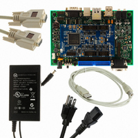
KIT - CDB5560 W/ Capture Plus II System
Manufacturer
Cirrus Logic Inc
Series
CapturePLUS™IIr
Specifications of CDK5560
Number Of Adc's
1
Number Of Bits
24
Sampling Rate (per Second)
50k
Data Interface
Serial
Inputs Per Adc
1 Differential
Input Range
±3 V
Power (typ) @ Conditions
90mW @ 2.5 V
Voltage Supply Source
Dual ±
Operating Temperature
-40°C ~ 85°C
Utilized Ic / Part
CS5560
Lead Free Status / RoHS Status
Contains lead / RoHS non-compliant
Other names
598-1277
CDK5560-1
CDK5560-1


RECOMMENDED OPERATING CONDITIONS
ABSOLUTE MAXIMUM RATINGS
Notes:
Recommended Operating Conditions indicate limits to which the device is functionally operational. Abso-
lute Maximum Ratings indicate limits beyond which permanent damage to the device may occur. The
Absolute Maximum Ratings are stress ratings only and the device should not be operated at these limits.
Operation at conditions beyond the Recommended Operating Conditions may affect device reliability, and
functional operation beyond Recommended Operating Conditions is not implied. Performance specifica-
tions are intended for the conditions specified for each table in the Characteristics and Specifications sec-
tion.
12
Single Analog Supply
DC Power Supplies:
Dual Analog Supplies
DC Power Supplies:
Analog Reference Voltage
DC Power Supplies:
Input Current, Any Pin Except Supplies
Analog Input Voltage
Digital Input Voltage
Storage Temperature
(VLR = 0V, see Note 15
(VLR = 0V
15. The logic supply can be any value VL – VLR = +1.71 to +3.465 volts as long as VLR ≥ V2- and VL ≤ 3.465 V.
16. The differential voltage reference magnitude is constrained by the V1+ or V1- supply magnitude.
17. V1+ = V2+; V1- = V2-
18. V1- = V2-
19. Transient currents of up to 100 mA will not cause SCR latch-up.
)
Parameter
Parameter
)
[V1+] – [V1-] (Note 17)
VL + [ |V1-| ] (Note 18)
(AIN and VREF pins)
[VREF+] – [VREF-]
(Note 19)
(Note 15)
(Note 15)
(Note 16)
WARNING:
5/4/09
V1+
V2+
V1+
V2+
V1-
V2-
V1-
V2-
Symbol
Symbol
V
VREF
V
T
I
V1+
V1+
V1+
V1+
V2-
V2-
V2-
V2-
IND
INA
IN
stg
-
-
(V1-) – 0.3
VLR – 0.3
+2.375
+2.375
-2.375
-2.375
Min
-65
4.75
4.75
Min
2.4
0
0
-
-
-
4.096
Typ
+2.5
+2.5
Typ
-2.5
-2.5
5.0
5.0
-
-
-
-
-
-
0
0
(V1+) + 0.3
VL + 0.3
+2.625
+2.625
-2.625
-2.625
Max
5.25
5.25
Max
±10
150
4.2
5.5
6.1
-
-
CS5560
DS713PP2
Unit
Unit
mA
V
V
V
V
V
V
V
V
V
°C
V
V
V
V
Related parts for CDK5560
Image
Part Number
Description
Manufacturer
Datasheet
Request
R

Part Number:
Description:
Development Kit
Manufacturer:
Cirrus Logic Inc
Datasheet:
Part Number:
Description:
Development Kit
Manufacturer:
Cirrus Logic Inc
Datasheet:


Part Number:
Description:
High-efficiency PFC + Fluorescent Lamp Driver Reference Design
Manufacturer:
Cirrus Logic Inc
Datasheet:
Part Number:
Description:
Development Kit
Manufacturer:
Cirrus Logic Inc
Datasheet:
Part Number:
Description:
Development Kit
Manufacturer:
Cirrus Logic Inc
Datasheet:

Part Number:
Description:
Development Kit
Manufacturer:
Cirrus Logic Inc
Datasheet:
Part Number:
Description:
Development Kit
Manufacturer:
Cirrus Logic Inc
Datasheet:
Part Number:
Description:
Development Kit
Manufacturer:
Cirrus Logic Inc
Datasheet:
Part Number:
Description:
Development Kit
Manufacturer:
Cirrus Logic Inc
Datasheet:

Part Number:
Description:
EVALUATION BOARD FOR CS8427
Manufacturer:
Cirrus Logic Inc
Datasheet:

Part Number:
Description:
BOARD EVAL FOR CS8416 RCVR
Manufacturer:
Cirrus Logic Inc
Datasheet:

Part Number:
Description:
EVALUATION BOARD FOR CS8420
Manufacturer:
Cirrus Logic Inc
Datasheet:

Part Number:
Description:
KIT DEVELOPMENT EP9315 ARM9
Manufacturer:
Cirrus Logic Inc
Datasheet:

Part Number:
Description:
KIT DEVELOPMENT EP9302 ARM9
Manufacturer:
Cirrus Logic Inc
Datasheet: