CDK5560 Cirrus Logic Inc, CDK5560 Datasheet - Page 5
CDK5560
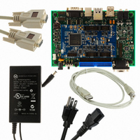
Manufacturer Part Number
CDK5560
Description
KIT - CDB5560 W/ Capture Plus II System
Manufacturer
Cirrus Logic Inc
Series
CapturePLUS™IIr
Specifications of CDK5560
Number Of Adc's
1
Number Of Bits
24
Sampling Rate (per Second)
50k
Data Interface
Serial
Inputs Per Adc
1 Differential
Input Range
±3 V
Power (typ) @ Conditions
90mW @ 2.5 V
Voltage Supply Source
Dual ±
Operating Temperature
-40°C ~ 85°C
Utilized Ic / Part
CS5560
Lead Free Status / RoHS Status
Contains lead / RoHS non-compliant
Other names
598-1277
CDK5560-1
CDK5560-1


ANALOG CHARACTERISTICS
V2- = -2.5 V, ±5%; VL -VLR = 3.3 V, ±5%; VREF = (VREF+) - (VREF-) = 4.096V; MCLK = 16 MHz; SMODE = VL.;
BUFEN = V1+ unless otherwise stated. Connected per
DS713PP2
Analog Input
Analog Input Range
Input Capacitance
CVF Current (Note 4)
Common Mode Rejection Ratio (CMRR)
Voltage Reference Input
Voltage Reference Input Range
(VREF+) – (VREF-)
Input Capacitance
CVF Current
Power Supplies
DC Power Supply Currents
Power Consumption
Power Supply Rejection
4.
5.
6.
the same voltage potential.
Measured using an input signal of 1 V DC.
For optimum performance, VREF+ should always be less than (V+) - 0.2 volts to prevent saturation of the VREF+ input buffer.
Tested with 100 mVP-P on any supply up to 2 kHz. V1+ and V2+ supplies at the same voltage potential, V1- and V2- supplies at
Parameter
VREF+ Buffer On (BUFEN = V+)
VREF+ Buffer Off (BUFEN = V-)
(Note 6)
Normal Operation Buffers On
AIN Buffer On (BUFEN = V+)
AIN Buffer Off (BUFEN = V-)
(CONTINUED)
V1+ , V2+ Supplies
V1-, V2- Supplies
5/4/09
Figure
Buffers Off
Unipolar
(Note 5)
Bipolar
VREF-
T
A
6.
I
I
I
= -40 to +85 °C; V1+ = V2+ = +2.5 V, ±5%; V1- =
V1
V2
VL
Min
116
2.4
60
60
-
-
-
-
-
-
-
-
-
-
-
-
0 to +VREF
4.096
±VREF
Typ
600
130
130
90
60
70
70
10
10
3
1
1
-
-
-
Max
106
4.2
1.8
0.6
19
90
-
-
-
-
-
-
-
-
-
-
CS5560
Unit
mW
mW
mA
mA
mA
mA
mA
nA
μA
dB
μA
dB
dB
pF
pF
V
V
V
5
Related parts for CDK5560
Image
Part Number
Description
Manufacturer
Datasheet
Request
R

Part Number:
Description:
Development Kit
Manufacturer:
Cirrus Logic Inc
Datasheet:
Part Number:
Description:
Development Kit
Manufacturer:
Cirrus Logic Inc
Datasheet:


Part Number:
Description:
High-efficiency PFC + Fluorescent Lamp Driver Reference Design
Manufacturer:
Cirrus Logic Inc
Datasheet:
Part Number:
Description:
Development Kit
Manufacturer:
Cirrus Logic Inc
Datasheet:
Part Number:
Description:
Development Kit
Manufacturer:
Cirrus Logic Inc
Datasheet:

Part Number:
Description:
Development Kit
Manufacturer:
Cirrus Logic Inc
Datasheet:
Part Number:
Description:
Development Kit
Manufacturer:
Cirrus Logic Inc
Datasheet:
Part Number:
Description:
Development Kit
Manufacturer:
Cirrus Logic Inc
Datasheet:
Part Number:
Description:
Development Kit
Manufacturer:
Cirrus Logic Inc
Datasheet:

Part Number:
Description:
EVALUATION BOARD FOR CS8427
Manufacturer:
Cirrus Logic Inc
Datasheet:

Part Number:
Description:
BOARD EVAL FOR CS8416 RCVR
Manufacturer:
Cirrus Logic Inc
Datasheet:

Part Number:
Description:
EVALUATION BOARD FOR CS8420
Manufacturer:
Cirrus Logic Inc
Datasheet:

Part Number:
Description:
KIT DEVELOPMENT EP9315 ARM9
Manufacturer:
Cirrus Logic Inc
Datasheet:

Part Number:
Description:
KIT DEVELOPMENT EP9302 ARM9
Manufacturer:
Cirrus Logic Inc
Datasheet: