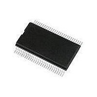
PCF8579TD NXP Semiconductors, PCF8579TD Datasheet - Page 8

PCF8579TD
Manufacturer Part Number
PCF8579TD
Description
LCD Drivers LCD DRVR DOT MATRIX
Manufacturer
NXP Semiconductors
Datasheet
1.PCF8579T1112.pdf
(41 pages)
Specifications of PCF8579TD
Maximum Clock Frequency
10 KHz
Operating Supply Voltage
2.5 V to 6 V
Maximum Power Dissipation
400 mW
Package / Case
VSO-56
Maximum Supply Current
20 uA
Lead Free Status / RoHS Status
Lead free / RoHS Compliant
Other names
PCF8579T/1,112
NXP Semiconductors
PCF8579_5
Product data sheet
8.2 Multiplexed LCD bias generation
V
V
Remark: Do not transfer data on the I
reset action to complete.
The bias levels required to produce maximum contrast depend on the multiplex rate and
the LCD threshold voltage (V
LCD exhibits 10 % contrast.
the discrimination ratios (D) for the different multiplex rates as functions of V
The RMS on-state voltage (V
and the RMS off-state voltage (V
where the values for n are determined by the multiplex rate (1:n). Valid values for n are:
Table 4.
V
Bias ratios
------------- -
V
------------- -
V
------------- -
V
------------- -
V
oper
off RMS
on RMS
n = 8 for 1:8 multiplex
n = 16 for 1:16 multiplex
n = 24 for 1:24 multiplex
n = 32 for 1:32 multiplex
V
V
V
V
oper
oper
oper
oper
2
3
4
5
=
V
=
=
DD
Optimum LCD voltages
V
V
–
oper
oper
V
LCD
1
-- -
n
------------------------------ -
Multiplex rate
1:8
0.739
0.522
0.478
0.261
2
+
n
------------------------
n
n 1
n
Rev. 05 — 11 May 2009
n 1
–
+
n
–
+
1
1
Table 4
2
th
on(RMS)
). V
off(RMS)
th
LCD column driver for dot matrix graphic displays
is typically defined as the RMS voltage at which the
) for the LCD is calculated with the equation
1:16
0.800
0.600
0.400
0.200
shows the optimum voltage bias levels and
2
C-bus for at least 1 ms after power-on to allow the
) with the equation
1:24
0.830
0.661
0.339
0.170
PCF8579
© NXP B.V. 2009. All rights reserved.
1:32
0.850
0.700
0.300
0.150
oper
.
Table 5
8 of 41
(1)
(2)
(3)


