ST7MDT1-DVP2/US STMicroelectronics, ST7MDT1-DVP2/US Datasheet - Page 58
ST7MDT1-DVP2/US
Manufacturer Part Number
ST7MDT1-DVP2/US
Description
MCU, MPU & DSP Development Tools ST7 Development Kit
Manufacturer
STMicroelectronics
Datasheet
1.ST7MDT1-DVP2US.pdf
(74 pages)
Specifications of ST7MDT1-DVP2/US
Processor To Be Evaluated
ST72254
Interface Type
Parallel Port
Lead Free Status / RoHS Status
Lead free / RoHS Compliant


5 - Hardware Features
58/74
Function/Feature
Ports A7, A5, A3,
Analog to Digital
A2, A1, A0
Stack Size
Emulation
Converter
Target Device
Group 2
Group 2
Group 2
Group
For those devices in Group 2, the Analog to Digital
Converter cell will have a longer conversion time
in emulation than for the actual target device.
While the Development Kit allows you to set a
Push/Pull configuration for these ports, this is not
a supported feature on actual Group 2 target
devices.
The emulation chip’s stack is located between
addresses 0x100 and 0x17F. While those target
devices in Group 1 also have the stack in this same
location, the target devices in Group 2 have their
stack located between addresses 0x140 and
0x17F.
This discrepancy between the emulation chip and
Group 2 target devices has the following
repercussions during an emulation/debugging
session:
After a “Stack Underflow” break, the stack pointer
(i.e. the SP register) will indicate the address 0x100
(and not 0x140 as would occur with the actual
target device).
After a “Stack Overflow” break, the stack pointer
(i.e. the SP register) will indicate the address
0x13F (and not 0x17F as would occur with the
actual target device).
Note that if a Stack Overflow break is not validated,
any overflow of the stack will erase user variables
(if any) situated between addresses 0x100 and
0x13F inclusive.
Limitation or Discrepancy
ST7MDT1-DVP2 User Manual
Related parts for ST7MDT1-DVP2/US
Image
Part Number
Description
Manufacturer
Datasheet
Request
R

Part Number:
Description:
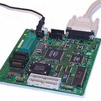
BOARD PROGRAMMING ST7
Manufacturer:
STMicroelectronics
Datasheet:
Part Number:
Description:
MCU, MPU & DSP Development Tools ST7 Evaluation Board
Manufacturer:
STMicroelectronics
Part Number:
Description:
MCU, MPU & DSP Development Tools ST7 Developmnt Board
Manufacturer:
STMicroelectronics

Part Number:
Description:
MCU, MPU & DSP Development Tools ST7 Emulator Board
Manufacturer:
STMicroelectronics
Part Number:
Description:
STMicroelectronics [RIPPLE-CARRY BINARY COUNTER/DIVIDERS]
Manufacturer:
STMicroelectronics
Datasheet:
Part Number:
Description:
STMicroelectronics [LIQUID-CRYSTAL DISPLAY DRIVERS]
Manufacturer:
STMicroelectronics
Datasheet:

Part Number:
Description:
BOARD EVAL FOR MEMS SENSORS
Manufacturer:
STMicroelectronics
Datasheet:
Part Number:
Description:
NPN TRANSISTOR POWER MODULE
Manufacturer:
STMicroelectronics
Datasheet:
Part Number:
Description:
TURBOSWITCH ULTRA-FAST HIGH VOLTAGE DIODE
Manufacturer:
STMicroelectronics
Datasheet:
Part Number:
Description:
Manufacturer:
STMicroelectronics
Datasheet:
Part Number:
Description:
DIODE / SCR MODULE
Manufacturer:
STMicroelectronics
Datasheet:
Part Number:
Description:
DIODE / SCR MODULE
Manufacturer:
STMicroelectronics
Datasheet: