A1360LKTTN-T Allegro Microsystems Inc, A1360LKTTN-T Datasheet - Page 10
A1360LKTTN-T
Manufacturer Part Number
A1360LKTTN-T
Description
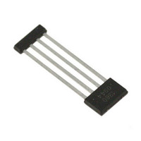
IC,HALL-EFFECT SENSOR,SINGLE-ENDED,BICMOS,SIP,4PIN,PLASTIC
Manufacturer
Allegro Microsystems Inc
Type
Linear - Unipolar, Bipolarr
Datasheet
1.A1360LKTTN-T.pdf
(25 pages)
Specifications of A1360LKTTN-T
Sensing Range
0.7mV/G ~ 1.4mV/G
Voltage - Supply
4.5 V ~ 5.5 V
Current - Supply
12mA
Current - Output (max)
10mA
Output Type
Analog, Ratiometric
Features
Programmable
Operating Temperature
-40°C ~ 150°C
Package / Case
4-SIP
Lead Free Status / RoHS Status
Lead free / RoHS Compliant
Other names
620-1233-2


A1360, A1361,
and A1362
Delay to Clamp
to overshoot its steady state value. The Delay to Clamp, t
defined as: the time it takes for the output voltage to settle within
±1% of its steady state value, after initially passing through its
steady state voltage, as shown in the following chart.
Quiescent Voltage Output
magnetic field: B = 0 G), the output, V
to the supply voltage, V
of V
Guaranteed Quiescent Voltage Output Range
voltage output, V
value of 2.5 V, within the guaranteed quiescent voltage range
limits: V
programming range for V
the initial, V
setting V
CC
V
CLP(HIGH)
and ambient temperature, T
OUT(Q)
OUT(Q)
Distribution for
V
V
OUT(Q)init
OUT(Q)init
V
OUT(Q)init
0
(min) and V
, as shown in the following diagram.
A large magnetic input step may cause the clamp
OUT(Q)
(typ)
t
t
Note: Times apply to both high clamp
(shown) and low clamp.
t
, and the maximum programming code for
1
2
1
= time at which output voltage initially
= time at which output voltage settles to
V
CC
, can be programmed around its nominal
reaches steady state clamp voltage
within 1% of steady state clamp voltage
OUT(Q)
Guaranteed Output
OUT(Q)
t
, throughout the entire operating ranges
CLP
Range, V
OUT(Q)
Programming
In the quiescent state (no significant
(min)
falls within the distributions of
t
(max). The available guaranteed
2
Adjustable Bandwidth (50 kHz Maximum) and Analog Output
A
OUT(Q)
V
Low-Noise Programmable Linear Hall Effect Sensor ICs with
.
OUT(Q)
Magnetic Input
OUT(Q)
(max)
Max Code V
Distribution for
V
, has a constant ratio
OUT
The quiescent
OUT(Q)
CLP
t
, is
Average Quiescent Voltage Output Step Size
escent voltage output step size for a single device is determined
using the following calculation:
where:
Quiescent Voltage Output Programming Resolution
programming resolution for any device is half of its programming
step size. Therefore, the typical programming resolution will be:
Quiescent Voltage Output Drift Through Temperature Range
Due to internal component tolerances and thermal considerations,
the quiescent voltage output, V
value over the operating ambient temperature, T
of specification, the Quiescent Voltage Output Drift Through
Temperature Range, ∆V
V
of V
values.
Sensitivity
pendicular to the branded surface of the package face, increases
the output voltage from its quiescent value toward the supply
voltage rail. The amount of the output voltage increase is propor-
tional to the magnitude of the magnetic field applied. Conversely,
the application of a north polarity field decreases the output
voltage from its quiescent value. This proportionality is specified
as the magnetic sensitivity, Sens (mV/G), of the device, and it is
defined for bipolar devices as:
and for unipolar devices as:
where BPOS and BNEG are two magnetic fields with opposite
polarities.
n is the number of available programming bits in the trim range,
2
range, and
V
OUT(Q)
n
OUT(Q)maxcode
–1 is the value of the maximum programming code in the
OUT(Q)(TA)
Err
, should be calculated using the actual measured values
PGVOUT(Q)
Step
∆V
The presence of a south polarity magnetic field, per-
OUT(Q)
and V
VOUT(Q)
Sens =
Sens =
is the quiescent voltage output at code 2
(typ) = 0.5 × Step
OUT(Q)(25°C)
=
V
OUT(Q)
=
OUT(Q)(TA)
V
OUT(BPOS)
V
115 Northeast Cutoff
1.508.853.5000; www.allegromicro.com
Allegro MicroSystems, Inc.
Worcester, Massachusetts 01615-0036 U.S.A.
OUT(Q)maxcode
V
BPOS – BNEG
OUT(BPOS)
OUT(Q)
(mV), is defined as:
, rather than programming target
BPOS
–V
– V
2
, may drift from its nominal
OUT(Q)(25°C)
n
–1
OUT(BNEG)
– V
VOUT(Q)
–V
OUT(Q)
OUT(Q)init
A
The average qui-
(typ)
. For purposes
.
,
,
.
The
.
n
–1.
(1)
(3)
(4)
(5)
(2)
10
Related parts for A1360LKTTN-T
Image
Part Number
Description
Manufacturer
Datasheet
Request
R

Part Number:
Description:
Manufacturer:
Allegro Micro Systems, Inc.
Datasheet:

Part Number:
Description:
CONN RECEPT CPC 4POS REV SER 1
Manufacturer:
Tyco Electronics
Datasheet:

Part Number:
Description:
IC, HALL EFFECT SENSOR, Linear, SOIC-8
Manufacturer:
Allegro Microsystems Inc
Datasheet:
Part Number:
Description:
IC, HALL EFFECT SENSOR, Linear, SOIC-8
Manufacturer:
Allegro Microsystems Inc
Datasheet:
Part Number:
Description:
IC, HALL EFFECT SENSOR, Linear, SOIC-8
Manufacturer:
Allegro Microsystems Inc
Datasheet:

Part Number:
Description:
IC SWITCH INTERFACE 2CHAN 8-SOIC
Manufacturer:
Allegro Microsystems Inc
Datasheet:

Part Number:
Description:
IC SMOKE DETECTOR ION 16-DIP
Manufacturer:
Allegro Microsystems Inc
Datasheet:
Part Number:
Description:
IC SMOKE DETECTOR ION 16-DIP
Manufacturer:
Allegro Microsystems Inc
Datasheet:
Part Number:
Description:
IC SMOKE DETECTOR ION 16-DIP
Manufacturer:
Allegro Microsystems Inc
Datasheet:
Part Number:
Description:
IC SMOKE DETECTOR PHOTO 16-DIP
Manufacturer:
Allegro Microsystems Inc
Datasheet:
Part Number:
Description:
IC SMOKE DETECTOR ION 16-DIP
Manufacturer:
Allegro Microsystems Inc
Datasheet:
Part Number:
Description:
IC SMOKE DETECTOR PHOTO 16-DIP
Manufacturer:
Allegro Microsystems Inc
Datasheet:
Part Number:
Description:
IC SMOKE DETECTOR PHOTO 16-DIP
Manufacturer:
Allegro Microsystems Inc
Datasheet:
Part Number:
Description:
IC SMOKE DETECTOR ION 16-DIP
Manufacturer:
Allegro Microsystems Inc
Datasheet:
Part Number:
Description:
IC SMOKE DETECTOR PHOTO 16-SOIC
Manufacturer:
Allegro Microsystems Inc
Datasheet: