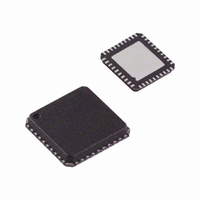
AD5412ACPZ-REEL7 Analog Devices Inc, AD5412ACPZ-REEL7 Datasheet - Page 10

AD5412ACPZ-REEL7
Manufacturer Part Number
AD5412ACPZ-REEL7
Description
12Bit 1V, I Out DAC
Manufacturer
Analog Devices Inc
Datasheet
1.AD5412ACPZ-REEL7.pdf
(40 pages)
Specifications of AD5412ACPZ-REEL7
Design Resources
Simplified 12-Bit Voltage and 4 mA-to-20 mA Output Solution Using AD5412 (CN0097)
Settling Time
25µs
Number Of Bits
12
Data Interface
MICROWIRE™, Serial, SPI™
Number Of Converters
1
Voltage Supply Source
Analog and Digital, Dual ±
Power Dissipation (max)
128mW
Operating Temperature
-40°C ~ 85°C
Mounting Type
Surface Mount
Package / Case
40-LFCSP
Number Of Channels
1
Resolution
12b
Conversion Rate
40KSPS
Interface Type
SER 3W SPI QSPI UW
Single Supply Voltage (typ)
12/15/18/24/28V
Architecture
R-2R
Power Supply Requirement
Single/Dual
Output Type
Current/Voltage
Single Supply Voltage (min)
10.8V
Single Supply Voltage (max)
40V
Dual Supply Voltage (min)
0/10.8V
Dual Supply Voltage (max)
-26.4/40V
Operating Temp Range
-40C to 85C
Operating Temperature Classification
Industrial
Mounting
Surface Mount
Pin Count
40
Lead Free Status / RoHS Status
Lead free / RoHS Compliant
Lead Free Status / RoHS Status
Lead free / RoHS Compliant
Other names
AD5412ACPZ-REEL7TR
Available stocks
Company
Part Number
Manufacturer
Quantity
Price
Company:
Part Number:
AD5412ACPZ-REEL7
Manufacturer:
Aptina
Quantity:
1 500
AD5412/AD5422
ABSOLUTE MAXIMUM RATINGS
T
80 mA do not cause SCR latch-up.
Table 5.
Parameter
AV
AV
AV
DV
Digital Inputs to GND
Digital Outputs to GND
REFIN/REFOUT to GND
V
I
Operating Temperature Range (T
Storage Temperature Range
Junction Temperature (T
24-Lead TSSOP Package
40-Lead LFCSP Package
Power Dissipation
Lead Temperature
ESD (Human Body Model)
1
OUT
Power dissipated on chip must be derated to keep the junction temperature
below 125°C, assuming that the maximum power dissipation condition is
sourcing 24 mA into GND from I
OUT
A
Industrial
θ
θ
Soldering
DD
SS
DD
CC
= 25°C, unless otherwise noted. Transient currents of up to
to GND
JA
JA
to GND
to GND
to GND
to AV
to GND
Thermal Impedance
Thermal Impedance
SS
1
J
max)
OUT
with a 4 mA on-chip current.
A
)
Rating
−0.3 V to +48 V
+0.3 V to −28 V
−0.3 V to +60 V
−0.3 V to +7 V
−0.3 V to DV
−0.3 V to DV
−0.3 V to +7 V
AV
−0.3 V to AV
−40°C to +85°C
−65°C to +150°C
125°C
42°C/W
28°C/W
(T
JEDEC industry standard
J-STD-020
2 kV
(whichever is less)
(whichever is less)
J
SS
max – T
to AV
DD
A
)/θ
DD
CC
CC
JA
+ 0.3 V or 7 V
+ 0.3 V or 7 V
Rev. C | Page 10 of 40
Stresses above those listed under Absolute Maximum Ratings
may cause permanent damage to the device. This is a stress
rating only; functional operation of the device at these or any
other conditions above those indicated in the operational
section of this specification is not implied. Exposure to absolute
maximum rating conditions for extended periods may affect
device reliability.
ESD CAUTION


