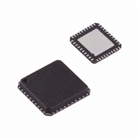
AD5412ACPZ-REEL7 Analog Devices Inc, AD5412ACPZ-REEL7 Datasheet - Page 29

AD5412ACPZ-REEL7
Manufacturer Part Number
AD5412ACPZ-REEL7
Description
12Bit 1V, I Out DAC
Manufacturer
Analog Devices Inc
Datasheet
1.AD5412ACPZ-REEL7.pdf
(40 pages)
Specifications of AD5412ACPZ-REEL7
Design Resources
Simplified 12-Bit Voltage and 4 mA-to-20 mA Output Solution Using AD5412 (CN0097)
Settling Time
25µs
Number Of Bits
12
Data Interface
MICROWIRE™, Serial, SPI™
Number Of Converters
1
Voltage Supply Source
Analog and Digital, Dual ±
Power Dissipation (max)
128mW
Operating Temperature
-40°C ~ 85°C
Mounting Type
Surface Mount
Package / Case
40-LFCSP
Number Of Channels
1
Resolution
12b
Conversion Rate
40KSPS
Interface Type
SER 3W SPI QSPI UW
Single Supply Voltage (typ)
12/15/18/24/28V
Architecture
R-2R
Power Supply Requirement
Single/Dual
Output Type
Current/Voltage
Single Supply Voltage (min)
10.8V
Single Supply Voltage (max)
40V
Dual Supply Voltage (min)
0/10.8V
Dual Supply Voltage (max)
-26.4/40V
Operating Temp Range
-40C to 85C
Operating Temperature Classification
Industrial
Mounting
Surface Mount
Pin Count
40
Lead Free Status / RoHS Status
Lead free / RoHS Compliant
Lead Free Status / RoHS Status
Lead free / RoHS Compliant
Other names
AD5412ACPZ-REEL7TR
Available stocks
Company
Part Number
Manufacturer
Quantity
Price
Company:
Part Number:
AD5412ACPZ-REEL7
Manufacturer:
Aptina
Quantity:
1 500
DATA REGISTER
The data register is addressed by setting the address word of the input shift register to 0x01. The data to be written to the data register is
entered in the D15 to D4 positions for the AD5412 and the D15 to D0 positions for the AD5422, as shown in Table 12 and Table 13.
Table 12. Programming the AD5412 Data Register
MSB
D15
Table 13. Programming the AD5422 Data Register
MSB
D15
CONTROL REGISTER
The control register is addressed by setting the address word of the input shift register to 0x55. The data to be written to the control
register is entered in the D15 to D0 positions, as shown in Table 14. The control register functions are shown in Table 15.
Table 14. Programming the Control Register
Table 15. Control Register Functions
Option
CLRSEL
OVRRNG
REXT
OUTEN
SR clock
SR step
SREN
DCEN
R2, R1, R0
Table 16. Output Range Options
R2
0
0
0
0
1
1
1
CLRSEL
MSB
D15
D14
D14
OVRRNG
D14
R1
0
0
1
1
0
1
1
D13
D13
REXT
D13
D12
D12
Description
See Table 21 for a description of the CLRSEL operation.
Setting this bit increases the voltage output range by 10% (see the AD5412/AD5422 Features section).
Setting this bit selects the external current setting resistor (see the AD5412/AD5422 Features section).
Output enable. This bit must be set to enable the outputs. The range bits select which output is functional.
Digital slew rate control (see the AD5412/AD5422 Features section).
Digital slew rate control (see the AD5412/AD5422 Features section).
Digital slew rate control enable.
Daisy chain enable.
Output range select (see Table 16).
R0
0
1
0
1
1
0
1
OUTEN
D12
D11
D11
12-bit data-word
D11
D10
D10
Output Range Selected
0 V to 5 V voltage range
0 V to 10 V voltage range
±5 V voltage range
±10 V voltage range
4 mA to 20 mA current range
0 mA to 20 mA current range
0 mA to 24 mA current range
D10
SR clock
D9
D9
Rev. C | Page 29 of 40
16-bit data-word
D9
D8
D8
D8
D7
D7
D7
D6
D6
SR step
D6
D5
D5
D5
D4
D4
SREN
D4
D3
D3
X
DCEN
D3
AD5412/AD5422
D2
D2
X
D2
R2
D1
D1
X
D1
R1
LSB
D0
LSB
D0
LSB
D0
X
R0


