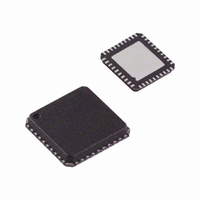
AD5412ACPZ-REEL7 Analog Devices Inc, AD5412ACPZ-REEL7 Datasheet - Page 27

AD5412ACPZ-REEL7
Manufacturer Part Number
AD5412ACPZ-REEL7
Description
12Bit 1V, I Out DAC
Manufacturer
Analog Devices Inc
Datasheet
1.AD5412ACPZ-REEL7.pdf
(40 pages)
Specifications of AD5412ACPZ-REEL7
Design Resources
Simplified 12-Bit Voltage and 4 mA-to-20 mA Output Solution Using AD5412 (CN0097)
Settling Time
25µs
Number Of Bits
12
Data Interface
MICROWIRE™, Serial, SPI™
Number Of Converters
1
Voltage Supply Source
Analog and Digital, Dual ±
Power Dissipation (max)
128mW
Operating Temperature
-40°C ~ 85°C
Mounting Type
Surface Mount
Package / Case
40-LFCSP
Number Of Channels
1
Resolution
12b
Conversion Rate
40KSPS
Interface Type
SER 3W SPI QSPI UW
Single Supply Voltage (typ)
12/15/18/24/28V
Architecture
R-2R
Power Supply Requirement
Single/Dual
Output Type
Current/Voltage
Single Supply Voltage (min)
10.8V
Single Supply Voltage (max)
40V
Dual Supply Voltage (min)
0/10.8V
Dual Supply Voltage (max)
-26.4/40V
Operating Temp Range
-40C to 85C
Operating Temperature Classification
Industrial
Mounting
Surface Mount
Pin Count
40
Lead Free Status / RoHS Status
Lead free / RoHS Compliant
Lead Free Status / RoHS Status
Lead free / RoHS Compliant
Other names
AD5412ACPZ-REEL7TR
Available stocks
Company
Part Number
Manufacturer
Quantity
Price
Company:
Part Number:
AD5412ACPZ-REEL7
Manufacturer:
Aptina
Quantity:
1 500
SERIAL INTERFACE
The AD5412/AD5422 are controlled over a versatile 3-wire
serial interface that operates at clock rates of up to 30 MHz. It is
compatible with SPI, QSPI™, MICROWIRE, and DSP standards.
Input Shift Register
The input shift register is 24 bits wide. Data is loaded into the
device MSB first as a 24-bit word under the control of a serial
clock input, SCLK. Data is clocked in on the rising edge of
SCLK. The input register consists of eight address bits and
16 data bits, as shown in Table 7. The 24-bit word is uncondi-
tionally latched on the rising edge of the LATCH pin. Data
continues to be clocked in irrespective of the state of LATCH.
On the rising edge of LATCH, the data that is present in the
input register is latched; in other words, the last 24 bits to be
clocked in before the rising edge of LATCH is the data that is
latched. The timing diagram for this operation is shown in
Figure 2.
Table 7. Input Shift Register Format
MSB
D23 to D16
Address byte
Table 8. Address Byte Functions
Address Word
00000000
00000001
00000010
01010101
01010110
Standalone Operation
The serial interface works with both a continuous and noncon-
tinuous serial clock. A continuous SCLK source can be used
only if LATCH is taken high after the correct number of data
bits have been clocked in. In gated clock mode, a burst clock
containing the exact number of clock cycles must be used, and
LATCH must be taken high after the final clock to latch the
data. The rising edge of SCLK that clocks in the MSB of the
data-word marks the beginning of the write cycle. Exactly 24
rising clock edges must be applied to SCLK before LATCH is
brought high. If LATCH is brought high before the 24
SCLK edge, the data written is invalid. If more than 24 rising
SCLK edges are applied before LATCH is brought high, the
input data is also invalid.
Function
No operation (NOP)
Data register
Readback register value as per read address
(see Table 9)
Control register
Reset register
D15 to D0
Data-word
th
rising
LSB
Rev. C | Page 27 of 40
Daisy-Chain Operation
For systems that contain several devices, the SDO pin can be
used to daisy-chain the devices together as shown in Figure 66.
This daisy-chain mode can be useful in system diagnostics and
in reducing the number of serial interface lines. Daisy-chain
mode is enabled by setting the DCEN bit of the control register
to 1. The first rising edge of SCLK that clocks in the MSB of the
data-word marks the beginning of the write cycle. SCLK is
continuously applied to the input shift register. If more than 24
clock pulses are applied, the data ripples out of the shift register
and appears on the SDO line. This data is valid on the rising
edge of SCLK, having been clocked out on the previous falling
SCLK edge. By connecting the SDO of the first device to the
SDIN input of the next device in the chain, a multidevice
interface is constructed. Each device in the system requires
24 clock pulses. Therefore, the total number of clock cycles
must equal 24 × n, where n is the total number of AD5412/
AD5422 devices in the chain. When the serial transfer to all
devices is complete, LATCH is taken high. This latches the
input data in each device in the daisy chain. The serial clock can
be a continuous or a gated clock.
A continuous SCLK source can be used only if LATCH is taken
high after the correct number of clock cycles. In gated clock
mode, a burst clock containing the exact number of clock cycles
must be used, and LATCH must be taken high after the final
clock to latch the data (see Figure 4 for a timing diagram).
1
ADDITIONAL PINS OMITTED FOR CLARITY.
CONTROLLER
Figure 66. Daisy Chaining the AD5412/AD5422
SERIAL CLOCK
CONTROL OUT
DATA IN
DATA OUT
SDIN
SCLK
LATCH
SCLK
LATCH
SCLK
LATCH
AD5412/AD5422
AD5422
AD5422
AD5422
AD5412/
AD5412/
AD5412/
SDIN
SDIN
SDO
SDO
SDO
1
1
1


