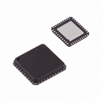
AD5412ACPZ-REEL7 Analog Devices Inc, AD5412ACPZ-REEL7 Datasheet - Page 28

AD5412ACPZ-REEL7
Manufacturer Part Number
AD5412ACPZ-REEL7
Description
12Bit 1V, I Out DAC
Manufacturer
Analog Devices Inc
Datasheet
1.AD5412ACPZ-REEL7.pdf
(40 pages)
Specifications of AD5412ACPZ-REEL7
Design Resources
Simplified 12-Bit Voltage and 4 mA-to-20 mA Output Solution Using AD5412 (CN0097)
Settling Time
25µs
Number Of Bits
12
Data Interface
MICROWIRE™, Serial, SPI™
Number Of Converters
1
Voltage Supply Source
Analog and Digital, Dual ±
Power Dissipation (max)
128mW
Operating Temperature
-40°C ~ 85°C
Mounting Type
Surface Mount
Package / Case
40-LFCSP
Number Of Channels
1
Resolution
12b
Conversion Rate
40KSPS
Interface Type
SER 3W SPI QSPI UW
Single Supply Voltage (typ)
12/15/18/24/28V
Architecture
R-2R
Power Supply Requirement
Single/Dual
Output Type
Current/Voltage
Single Supply Voltage (min)
10.8V
Single Supply Voltage (max)
40V
Dual Supply Voltage (min)
0/10.8V
Dual Supply Voltage (max)
-26.4/40V
Operating Temp Range
-40C to 85C
Operating Temperature Classification
Industrial
Mounting
Surface Mount
Pin Count
40
Lead Free Status / RoHS Status
Lead free / RoHS Compliant
Lead Free Status / RoHS Status
Lead free / RoHS Compliant
Other names
AD5412ACPZ-REEL7TR
Available stocks
Company
Part Number
Manufacturer
Quantity
Price
Company:
Part Number:
AD5412ACPZ-REEL7
Manufacturer:
Aptina
Quantity:
1 500
AD5412/AD5422
Readback Operation
Readback mode is invoked by setting the address byte and
read address when writing to the input register (see Table 9 and
Table 11). The next write to the AD5412/AD5422 should be a
NOP command, which clocks out the data from the previously
addressed register as shown in Figure 3.
By default the SDO pin is disabled after having addressed the
AD5412/AD5422 for a read operation; a rising edge on LATCH
enables the SDO pin in anticipation of data being clocked out.
After the data has been clocked out on SDO, a rising edge on
LATCH disables (tristate) the SDO pin. To read back the data
register, for example, implement the following sequence:
1.
2.
Table 9. Read Address Decoding
Read Address
00
01
10
POWER-ON STATE
During power-on of the AD5412/AD5422, the power-on-reset
circuit ensures that all registers are loaded with zero-code. As
such, both outputs are disabled; that is, the V
are in tristate. The +V
through a 40 kΩ resistor. Therefore, if the V
are connected together, V
through a 40 kΩ resistor. Also upon power-on, internal
calibration registers are read, and the data is applied to internal
calibration circuitry. For a reliable read operation, there must be
sufficient voltage on the AV
triggered by the DV
the DV
AV
enabled, the supplies should be powered up at a rate greater
than, typically, 500 V/sec or 24 V/50 ms. If this cannot be
achieved, issue a reset command to the AD5412/AD5422 after
power-on; this performs a power-on-reset event, reading the
Table 11. Input Shift Register Contents for a Read Operation
MSB
D23
0
1
X = don’t care.
DD
Write 0x020001 to the input register. This configures the
part for read mode with the data register selected.
Follow this with a second write: a NOP condition, which is
0x000000. During this write, the data from the register is
clocked out on the SDO line.
are powered up simultaneously or the internal DV
CC
D22
0
supply after the AV
D21
0
CC
SENSE
power supply powering up. Powering up
OUT
D20
0
pin is internally connected to ground
DD
Function
Read status register
Read data register
Read control register
DD
is effectively clamped to ground
supply when the read event is
supply ensures this. If DV
D19
0
D18
0
OUT
OUT
and +V
and I
D17
1
OUT
SENSE
CC
pins
CC
is
D16
0
pins
and
Rev. C | Page 28 of 40
calibration registers and ensures specified operation of the
AD5412/AD5422.
Voltage Output
For a unipolar voltage output range, the output voltage can be
expressed as
For a bipolar voltage output range, the output voltage can be
expressed as
where:
D is the decimal equivalent of the code loaded to the DAC.
N is the bit resolution of the DAC.
V
Gain is an internal gain whose value depends on the output
range selected by the user as shown in Table 10.
Table 10. Internal Gain Value
Output Range
+5 V
+10 V
±5 V
±10 V
Current Output
For the 0 mA to 20 mA, 0 mA to 24 mA, and 4 mA to 20 mA
current output ranges, the output current is respectively
expressed as
where:
D is the decimal equivalent of the code loaded to the DAC.
N is the bit resolution of the DAC.
REFIN
V
V
I
I
I
is the reference voltage applied at the REFIN pin.
OUT
OUT
OUT
OUT
OUT
=
=
=
=
=
⎡
⎢
⎣
⎡
⎢
⎣
⎡
⎢
⎣
V
V
16
20
24
REFIN
REFIN
D15 to D2
2
2
2
mA
mA
mA
N
N
N
X
×
×
1
⎤
⎥
⎦
⎤
⎥
⎦
⎤
⎥
⎦
Gain
Gain
×
×
×
D
D
D
+
⎡
⎢ ⎣
⎡
⎢ ⎣
2
2
4
D
D
N
N
mA
⎤
⎥ ⎦
⎤
⎥ ⎦
−
Gain
Gain Value
1
2
2
4
×
2
V
REFIN
D1
Read address
LSB
D0


