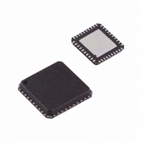
AD5412ACPZ-REEL7 Analog Devices Inc, AD5412ACPZ-REEL7 Datasheet - Page 12

AD5412ACPZ-REEL7
Manufacturer Part Number
AD5412ACPZ-REEL7
Description
12Bit 1V, I Out DAC
Manufacturer
Analog Devices Inc
Datasheet
1.AD5412ACPZ-REEL7.pdf
(40 pages)
Specifications of AD5412ACPZ-REEL7
Design Resources
Simplified 12-Bit Voltage and 4 mA-to-20 mA Output Solution Using AD5412 (CN0097)
Settling Time
25µs
Number Of Bits
12
Data Interface
MICROWIRE™, Serial, SPI™
Number Of Converters
1
Voltage Supply Source
Analog and Digital, Dual ±
Power Dissipation (max)
128mW
Operating Temperature
-40°C ~ 85°C
Mounting Type
Surface Mount
Package / Case
40-LFCSP
Number Of Channels
1
Resolution
12b
Conversion Rate
40KSPS
Interface Type
SER 3W SPI QSPI UW
Single Supply Voltage (typ)
12/15/18/24/28V
Architecture
R-2R
Power Supply Requirement
Single/Dual
Output Type
Current/Voltage
Single Supply Voltage (min)
10.8V
Single Supply Voltage (max)
40V
Dual Supply Voltage (min)
0/10.8V
Dual Supply Voltage (max)
-26.4/40V
Operating Temp Range
-40C to 85C
Operating Temperature Classification
Industrial
Mounting
Surface Mount
Pin Count
40
Lead Free Status / RoHS Status
Lead free / RoHS Compliant
Lead Free Status / RoHS Status
Lead free / RoHS Compliant
Other names
AD5412ACPZ-REEL7TR
Available stocks
Company
Part Number
Manufacturer
Quantity
Price
Company:
Part Number:
AD5412ACPZ-REEL7
Manufacturer:
Aptina
Quantity:
1 500
AD5412/AD5422
TSSOP
16
17
19
20
N/A
21
22
23
24
25 (EPAD)
Pin No.
LFCSP
33
34
23
24
26
27
28, 29
32
36
41 (EPAD)
Mnemonic
DV
SELECT
C
I
BOOST
CAP1, CAP2
V
+V
−V
AV
Exposed
paddle
OUT
OUT
COMP
SENSE
SENSE
DD
CC
Description
When connected to GND, this pin disables the internal supply, and an external supply
must be connected to the DV
supply. See the AD5412/AD5422 Features section.
Optional compensation capacitor connection for the voltage output buffer. Connecting
a 4 nF capacitor between this pin and the V
to 1 μF. It should be noted that the addition of this capacitor reduces the bandwidth of
the output amplifier, increasing the settling time.
Current Output Pin.
Optional External Transistor Connection. Connecting an external transistor reduces the
power dissipated in the AD5412/AD5422. See theAD5412/AD5422 Features section.
Connection for Optional Output Filtering Capacitor. See the AD5412/AD5422 Features
section.
Buffered Analog Output Voltage. The output amplifier is capable of directly driving a
1 kΩ, 2000 pF load.
Sense connection for the positive voltage output load connection.
Sense connection for the negative voltage output load connection.
Positive Analog Supply Pin. Voltage ranges from 10.8 V to 60 V.
Negative Analog Supply Pin. Voltage ranges from –3 V to –24 V. This paddle can be
connected to 0 V if the output voltage range is unipolar. The paddle can be left
electrically unconnected provided that a supply connection is made at the AV
recommended that the paddle be thermally connected to a copper plane for enhanced
thermal performance.
Rev. C | Page 12 of 40
CC
pin. Leave this pin unconnected to enable the internal
OUT
pin allows the voltage output to drive up
SS
pin. It is


