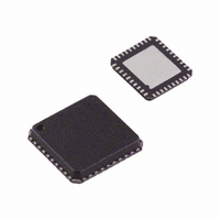
AD5412ACPZ-REEL7 Analog Devices Inc, AD5412ACPZ-REEL7 Datasheet - Page 26

AD5412ACPZ-REEL7
Manufacturer Part Number
AD5412ACPZ-REEL7
Description
12Bit 1V, I Out DAC
Manufacturer
Analog Devices Inc
Datasheet
1.AD5412ACPZ-REEL7.pdf
(40 pages)
Specifications of AD5412ACPZ-REEL7
Design Resources
Simplified 12-Bit Voltage and 4 mA-to-20 mA Output Solution Using AD5412 (CN0097)
Settling Time
25µs
Number Of Bits
12
Data Interface
MICROWIRE™, Serial, SPI™
Number Of Converters
1
Voltage Supply Source
Analog and Digital, Dual ±
Power Dissipation (max)
128mW
Operating Temperature
-40°C ~ 85°C
Mounting Type
Surface Mount
Package / Case
40-LFCSP
Number Of Channels
1
Resolution
12b
Conversion Rate
40KSPS
Interface Type
SER 3W SPI QSPI UW
Single Supply Voltage (typ)
12/15/18/24/28V
Architecture
R-2R
Power Supply Requirement
Single/Dual
Output Type
Current/Voltage
Single Supply Voltage (min)
10.8V
Single Supply Voltage (max)
40V
Dual Supply Voltage (min)
0/10.8V
Dual Supply Voltage (max)
-26.4/40V
Operating Temp Range
-40C to 85C
Operating Temperature Classification
Industrial
Mounting
Surface Mount
Pin Count
40
Lead Free Status / RoHS Status
Lead free / RoHS Compliant
Lead Free Status / RoHS Status
Lead free / RoHS Compliant
Other names
AD5412ACPZ-REEL7TR
Available stocks
Company
Part Number
Manufacturer
Quantity
Price
Company:
Part Number:
AD5412ACPZ-REEL7
Manufacturer:
Aptina
Quantity:
1 500
AD5412/AD5422
THEORY OF OPERATION
The AD5412/AD5422 are precision digital-to-current loop and
voltage output converters designed to meet the requirements of
industrial process control applications. They provide a high
precision, fully integrated, low cost single-chip solution for
generating current loop and unipolar/bipolar voltage outputs.
Current ranges are 0 mA to 20 mA, 0 mA to 24 mA, and 4 mA
to 20 mA; the voltage ranges available are 0 V to 5 V, ±5 V, 0 V
to 10 V, and ±10 V; a 10% overrange is available on all voltage
output ranges. The current and voltage outputs are available on
separate pins, and only one is active at any time. The desired
output configuration is user selectable via the control register.
ARCHITECTURE
The DAC core architecture of the AD5412/AD5422 consists
of two matched DAC sections. A simplified circuit diagram is
shown in Figure 63. The four MSBs of the 12-/16-bit data-word
are decoded to drive 15 switches, E1 to E15. Each of these switches
connects one of 15 matched resistors to either ground or the
reference buffer output. The remaining 8/12 bits of the data-
word drive the S0 to S7/S11 switches of an 8-/12-bit voltage
mode R-2R ladder network.
The voltage output from the DAC core is either converted to
a current (see Figure 64) which is then mirrored to the supply
rail so that the application simply sees a current source output
with respect to ground or it is buffered and scaled to output a
software selectable unipolar or bipolar voltage range (see
Figure 65). The current and voltage are output on separate
pins and cannot be output simultaneously.
2R
8-12 BIT R-2R LADDER
12-/16-BIT
Figure 64. Voltage-to-Current Conversion Circuitry
DAC
S0
2R
Figure 63. DAC Ladder Structure
2R
S1
A1
2R
S7/S11
FOUR MSBs DECODED INTO
T1
15 EQUAL SEGMENTS
R2
R
SET
2R
E1
A2
2R
E2
T2
AV
DD
R3
I
OUT
2R
E15
V
OUT
Rev. C | Page 26 of 40
Voltage Output Amplifier
The voltage output amplifier is capable of generating both
unipolar and bipolar output voltages. It is capable of driving
a load of 1 kΩ in parallel with 1 μF (with an external compen-
sation capacitor) to GND. The source and sink capabilities of
the output amplifier can be seen in Figure 35. The slew rate
is 1 V/μs with a full-scale settling time of 25 μs maximum (10 V
step). Figure 65 shows the voltage output driving a load, R
on top of a common-mode voltage (V
output module applications where a cable could possibly
become disconnected from +V
loop being broken and possibly resulting in large destructive
voltages on V
+V
2 kΩ and 5 kΩ to ensure the amplifier loop is kept closed. If
remote sensing of the load is not required, connect +V
directly to V
changing ranges on the voltage output, a glitch may occur. For
this reason, it is recommended that the output be disabled by
setting the OUTEN bit of the control register to logic low before
changing the output voltage range; this prevents a glitch from
occurring.
Driving Large Capacitive Loads
The voltage output amplifier is capable of driving capacitive
loads of up to 1 μF with the addition of a nonpolarized 4 nF
compensation capacitor between the C
Without the compensation capacitor, up to 20 nF capacitive
loads can be driven.
AD5412/AD5422
12-/16-BIT
SENSE
DAC
REFIN
and V
OUT
OUT
OUT
SCALING
RANGE
and connect −V
, include an optional resistor (R1) between
, as shown in Figure 65, of a value between
Figure 65. Voltage Output
+V
–V
SENSE
SENSE
SENSE
SENSE
V
OUT
, resulting in the amplifier
directly to GND. When
CM
COMP
) of −1 V to +3 V. In
R1
and V
–1V TO +3V
OUT
pins.
SENSE
V
CM
R
LOAD
LOAD
,


