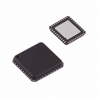
AD8195ACPZ-R7 Analog Devices Inc, AD8195ACPZ-R7 Datasheet

AD8195ACPZ-R7
Specifications of AD8195ACPZ-R7
Available stocks
Related parts for AD8195ACPZ-R7
AD8195ACPZ-R7 Summary of contents
Page 1
FEATURES 1 input, 1 output HDMI/DVI link Enables HDMI 1.3a-compliant front panel input 4 TMDS channels per link Supports 250 Mbps to 2.25 Gbps data rates Supports 25 MHz to 225 MHz pixel clocks Equalized inputs for operation with long ...
Page 2
AD8195 TABLE OF CONTENTS Features .............................................................................................. 1 Applications ....................................................................................... 1 General Description ......................................................................... 1 Functional Block Diagram .............................................................. 1 Typical Application ........................................................................... 1 Product Highlights ........................................................................... 1 Revision History ............................................................................... 2 Specifications ..................................................................................... 3 TMDS Performance Specifications ............................................ 3 Auxiliary ...
Page 3
SPECIFICATIONS T = 27°C, AVCC = 3.3 V, VTTI = 3.3 V, VTTO = 3.3 V, AMUXVCC = 5 V, VREF_IN = 5 V, VREF_OUT = 5 V, AVEE = 0 V, differential input A swing = 1000 mV, TMDS ...
Page 4
AD8195 AUXILIARY CHANNEL PERFORMANCE SPECIFICATIONS Table 2. Parameter Conditions/Comments DDC CHANNELS Input Capacitance bias = 2 voltage = 3 100 kHz AUX Input Low Voltage Input High Voltage ...
Page 5
ABSOLUTE MAXIMUM RATINGS Table 4. Parameter AVCC to AVEE VTTI VTTO AMUXVCC VREF_IN VREF_OUT Internal Power Dissipation High Speed Input Voltage High Speed Differential Input Voltage Parallel Control Input Voltage Storage Temperature Range Operating Temperature Range Junction Temperature ESD, Human ...
Page 6
AD8195 PIN CONFIGURATION AND FUNCTION DESCRIPTIONS Table 6. Pin Function Descriptions Pin No. Mnemonic 1 IN0 2 IP0 3 IN1 4 IP1 5 VTTI 6 IN2 7 IP2 8 IN3 9 IP3 10, 16, 22, 23, 25, 26, 30 AVCC ...
Page 7
Pin No. Mnemonic 33 VREF_OUT 34 SDA_OUT 35 SCL_OUT 36 VREF_IN 38 CEC_IN 39 SDA_IN 40 SCL_IN high speed low speed input output. 1 Type Description Reference DDC Output Side Pull-Up ...
Page 8
AD8195 TYPICAL PERFORMANCE CHARACTERISTICS T = 27°C, AVCC = 3.3 V, VTTI = 3.3 V, VTTO = 3.3 V, AVEE = 0 V, differential input swing = 1000 mV, pattern = PRBS 2 A data rate = 2.25 Gbps, TMDS ...
Page 9
T = 27°C, AVCC = 3.3 V, VTTI = 3.3 V, VTTO = 3.3 V, AVEE = 0 V, differential input swing = 1000 mV, pattern = PRBS 2 A data rate = 2.25 Gbps, TMDS outputs terminated with external ...
Page 10
AD8195 T = 27°C, AVCC = 3.3 V, VTTI = 3.3 V, VTTO = 3.3 V, AVEE = 0 V, differential input swing = 1000 mV, pattern = PRBS 2 A data rate = 2.25 Gbps, TMDS outputs terminated with ...
Page 11
T = 27°C, AVCC = 3.3 V, VTTI = 3.3 V, VTTO = 3.3 V, AVEE = 0 V, differential input swing = 1000 mV, pattern = PRBS 2 A data rate = 2.25 Gbps, TMDS outputs terminated with external ...
Page 12
AD8195 THEORY OF OPERATION INTRODUCTION The primary function of the AD8195 is to buffer a single (HDMI or DVI) link. The HDMI or DVI link consists of four differential, high speed channels and three auxiliary single-ended, low speed control signals. ...
Page 13
PREEMPHASIS The preemphasized TMDS outputs precompensate the trans- mitted signal to account for losses in systems with long cable runs. These long cable runs selectively attenuate the high frequency energy of the signal, leading to degraded transition times and eye ...
Page 14
AD8195 APPLICATIONS INFORMATION FRONT PANEL BUFFER FOR ADVANCED TV A front panel input provides easy access to an HDMI connector for connecting devices, such camcorder or video game console HDTV. In designs where the main ...
Page 15
HDMI CONNECTOR D2+ D2– D1+ D1– D0+ D0– CLK+ CLK– ESD PROTECTION 2kΩ (OPTIONAL) 5V 1kΩ HPD DDC_SCL DDC_SDA CEC EDID 0.01µF EEPROM CABLE LENGTHS AND EQUALIZATION The AD8195 offers equalization for the high speed inputs. ...
Page 16
AD8195 and transferred over a single-ended transmission line that does not need to have controlled impedance. The primary concern with laying out the auxiliary lines is ensuring that they conform 2 to the I C bus standard and do not ...
Page 17
TMDS Terminations The AD8195 provides internal 50 Ω single-ended terminations for all of its high speed inputs and outputs not necessary to include external termination resistors for the TMDS differential pairs on the PCB. The output termination resistors ...
Page 18
... OUTLINE DIMENSIONS PIN 1 INDICATOR 12° MAX 1.00 0.85 0.80 SEATING PLANE ORDERING GUIDE Temperature Model Range 1 AD8195ACPZ −40°C to +85°C 1 AD8195ACPZ-R7 −40°C to +85°C 1 AD8195-EVALZ RoHS Compliant Part. 6.00 BSC SQ 0.60 MAX 0.50 TOP BSC 5.75 VIEW BSC SQ 0.50 0.40 ...
Page 19
NOTES Rev Page AD8195 ...
Page 20
AD8195 NOTES Purchase of licensed 2 components of Analog Devices or one of its sublicensed Associated Companies conveys a license for the purchaser under the Philips Patent Rights to use these components ©2008 ...


