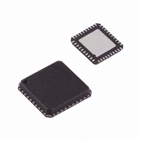
AD8195ACPZ-R7 Analog Devices Inc, AD8195ACPZ-R7 Datasheet - Page 15

AD8195ACPZ-R7
Manufacturer Part Number
AD8195ACPZ-R7
Description
Front Panel HDMI Buffer
Manufacturer
Analog Devices Inc
Datasheet
1.AD8195ACPZ-R7.pdf
(20 pages)
Specifications of AD8195ACPZ-R7
Function
Switch
Circuit
1 x 1:1
Voltage Supply Source
Single Supply
Voltage - Supply, Single/dual (±)
3 V ~ 3.6 V
Current - Supply
40mA
Operating Temperature
-40°C ~ 85°C
Mounting Type
Surface Mount
Package / Case
40-VFQFN, CSP Exposed Pad
Lead Free Status / RoHS Status
Lead free / RoHS Compliant
Available stocks
Company
Part Number
Manufacturer
Quantity
Price
Company:
Part Number:
AD8195ACPZ-R7
Manufacturer:
MITSUBISHI
Quantity:
101
CABLE LENGTHS AND EQUALIZATION
The AD8195 offers 12 dB of equalization for the high speed
inputs. The equalizer of the AD8195 is optimized for video
data rates of 2.25 Gbps and can equalize more than 20 meters of
24 AWG HDMI cable at the input for data rates corresponding to
the video format 1080p with deep color.
The length of cable that can be used in a typical HDMI/DVI
application depends on a large number of factors, including the
following:
•
•
•
•
TMDS OUTPUT RISE/FALL TIMES
The TMDS outputs of the AD8195 are designed for optimal
performance even when external components are connected,
such as external ESD protection, common-mode filters, and
the HDMI connector. In applications where the output of the
AD8195 is connected to an HDMI output connector, additional
ESD protection is recommended. The capacitance of the addi-
tional ESD protection circuits for the TMDS outputs should be
as low as possible. In a typical application, the output rise/fall
Cable quality: the quality of the cable in terms of conductor
wire gauge and shielding. Thicker conductors have lower
signal degradation per unit length.
Data rate: the data rate being sent over the cable. The signal
degradation of HDMI cables increases with data rate.
Edge rates: the edge rates of the source input. Slower input
edges result in more significant data eye closure at the end
of a cable.
Receiver sensitivity: the sensitivity of the terminating
receiver.
CONNECTOR
DDC_SDA
DDC_SCL
HDMI
CLK+
CLK–
HPD
CEC
D2+
D1+
D0+
D2–
D1–
D0–
5V
PROTECTION
(OPTIONAL)
ESD
0.01µF
1kΩ
2kΩ
EEPROM
EDID
1µF
TMDS
47kΩ
Figure 30. AD8195 Typical Application Simplified Schematic
TYPICAL EDID
PLACEMENT
0.01µF
47kΩ
10µF
AMUXVCC
Rev. 0 | Page 15 of 20
AMUXVCC
IPA3
INA3
IPA2
INA2
IPA1
INA1
IPA0
INA0
VREF_IN
SCL_IN
SDA_IN
CEC_IN
COMP
5V
AD8195
AVEE
AVCC, VTTI,
times are compliant with the HDMI 1.3a specification at the
output of the HDMI connector.
PCB LAYOUT GUIDELINES
The AD8195 is used to buffer two distinctly different types of
signals, both of which are required for HDMI and DVI video.
These signal groups require different treatment when laying
out a PCB.
The first group of signals carries the audiovisual (AV) data encoded
by a technique called transition minimized differential signaling
(TMDS) and, in the case of HDMI, is also encrypted according to
the high bandwidth digital copy protection (HDCP) standard.
HDMI/DVI video signals are differential, unidirectional, and
high speed (up to 2.25 Gbps). The channels that carry the video
data must have controlled impedance, be terminated at the
receiver, and be capable of operating up to at least 2.25 Gbps. It
is especially important to note that the differential traces that
carry the TMDS signals should be designed with a controlled
differential impedance of 100 Ω. The AD8195 provides single-
ended 50 Ω terminations on chip for both its inputs and
outputs. Transmitter termination is not fully specified by the
HDMI standard, but its inclusion improves the overall system
signal integrity.
The second group of signals consists of low speed auxiliary
control signals used for communication between a source and a
sink. These signals include the DDC bus (this is an I
to send EDID information and HDCP encryption keys between
the source and the sink) and the consumer electronics control
(CEC) line. These auxiliary signals are bidirectional, low speed,
VTTO
3.3V
VREF_OUT
SDA_OUT
CEC_OUT
SCL_OUT
ON3
ON2
ON1
ON0
OP3
OP2
OP1
OP0
AMUXVCC
3kΩ
6kΩ
3.3V OR 5V
TMDS
2kΩ
INTERCONNECT
2kΩ
CABLE OR PCB
EEPROM
D2+
D2–
D1+
D1–
D0+
D0–
CLK+
CLK–
DDC_SCL
DDC_SDA
EDID
CEC
MCU
RECEIVER
HDMI
0.01µF
OPTIONAL EDID
PLACEMENT
AD8195
2
C bus used


